 NIXIE CLOCK DIY

If wanna buy this kit,please check our store:
USB Powered
VFD48 Analog-style Unique Round VFD Clock
Assembly Instructions
Contents
Notice
Building it
Preparing
Step 1: USB Power In and MCU part
Step 2: RTC part
Step 3: Filament Driver part
Step 4: Negative High Voltage part circuit
Step 5: CDS and IR part
Step 6: VFD drive Chip
Step 7: First Testing
Step 8: Cleaning Circuit Board
Step 9: Buzzer part
Step 10: Buttons part
Step 11: Test the buttons, buzzer, and VFD panel
Step 12: Solder the VFD48 Panel
Step 12: Solder the Extras:
Circuit and PCB
Notice
For assembling the VFD48 clock you need to have the skill of soldering SMD components. We use a Hakko FX-888 Soldering Station (with CF2 Iron Head) and a Hot air blower station. We use 183℃(degree C)low melt temperature solder wire S60, 0.5mm(Dia.), Brand Almit.
For how to solder the SMD components, we recommend:
https://www.hakko.com/english/tip_selection/type_bc_c.html
https://www.hakkousa.com/video/
Please do not change any equipments of the KIT or you may not be able to get the clock working.
If already have the skill of soldering the SMD components, it is easy for you to assemble the clock, please check the circuit diagram carefully and follow the steps shown blow.
We do not recommend you to solder the components in random order or if it has problems you will need
more time for de-soldering and debug, we recommend you follow the steps in this instructions that you can do part test after finished each
step.
For more info & update, please visit HTTP://vfdclock.jimdo.com
Or contact us: zjjszhangf[at]gmail.com
Thanks for choosing our product.
Building it
Well, because of the circuit is module based and not very complicated, all you need to do is get all the components in the right position and make sure no short before you plug the power in. We will show the soldering steps blow.
Preparing
1. Please print out the PCB installation diagram by yourself, the Circuit diagram is no need for soldering job, print it or not depends on you(Note: May only have the paper circuit diagram in the KIT with no digital version provide.);
2. Check all the components in the kit bag, make sure nothing is missing (You can do this on a A4 white copy paper);
3. We recommend using a soldering station and small soldering tip for soldering this kit (we use F2 or CF2 type tip). If you have a hot air gun(or Hot air blower station) tool for soldering, that will be great. We recommend using ~180℃ type soldering tin for this job. Please do not use the high temperature soldering tin in this project, you may damage a lot of SMD components or the PCB;
Step 1: USB Power In and MCU part
Solder the [USB Power In] part first; This part contains a USB socket and a 1206 size RESETTABLE fuse.
For soldering the USB socket, we recommend solder the 5 middle Pins first, then flip the PCB to the other side and use long flat nose pliers to band the two fixed legs of the USB socket a little bit close then solder these two fixed legs.
Then solder the 1206 FUSE, usually in golden color with mark [4] on it, easy to find.
After soldering these two components, you can plug the USB power in and measure the fuse output pad to see if it has 5V output.
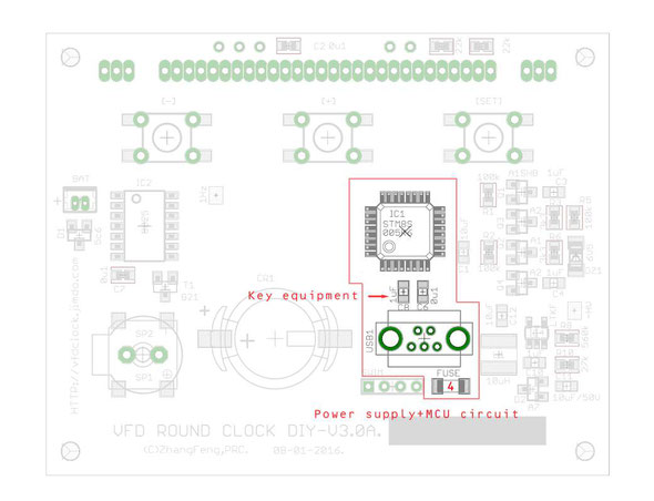
The next part of this step is soldering the main MCU chip, it is a LQFP32 package MCU with [105K6T6](or 005K6T6) mark on it. Please check the first legs position. For soldering the QFP stuff like this, we recommend that you use a short Polyimide Tape to glue the chip on the correct location of the PCB first, then solder one corner, if all fine, solder the other side pins in the next, then the rest sides' pins.
After finish soldering the MCU chip, double check all the pins, make sure no short. Then solder two capacitors blow the MCU chip(1uF and 0u1F), the 1uF one is the key component, must be installed or the MCU won't work.
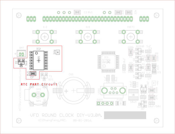
Step 2: RTC part
In this step, you need to solder the RTC (Real Time Clock) part components, it contains 3 components, the major one is the RX8025 RTC all in one chip in SOP14 package, it may have the mark RX8025AC or RX8025T mark on the surface depends on the kit's version. Please solder the chip in the correct direction, please control the iron's temperature, and solder it fast, and take care of the ESD(Electro Static Discharge) control.
Then solder the diodes D1 in sot-23 package with [5C6] mark and the 0u1F capacitor.
(*Please note that RX8025AC and RX8025T are not the compatible chips, if damaged the chip ,please use the same mark chip to replace).
You can try to plug the 5V USB power, if the RTC chip and the MCU in working, you can find the 1Hz(or 2Hz) signal in the 1Hz testing pad(you can use oscillograph if you have).
If you want, you can install the CR1220 Battery Socket too at this step, recommend to cut the left&right pads of the socket a little bit short for easy to solder.(Note: The straight metal pad part in the socket is the [+] pad, do not go invert;
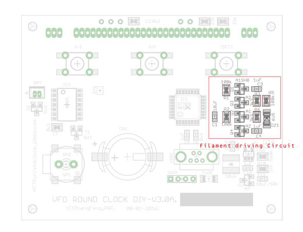
Step 3: Filament Driver part
Now we can solder the filament driver part components. This part of the circuit contains a H bridge which created by 4 MOSFETs and other components for EK level shift with the -HV part circuit.
This part of the MOSFETs components are SOTt23-3 MOSFET(A1SHB & A2SHB mark) and resistors and capacitors, please do not change the C3+C4(1uF/50V) capacitors value(only use the caps in the kit).
And it also contains a 6V5 Z-diode inside, usually in glass package with a round color bar(usually in blue or black) at the cathode side, easy to find, please solder it in the right direction.
After this step, you can plug the 5V USB power in ,then plug the VFD48 panel in (Please do not solder the panel at this time), press the panel a little bit to make sure the pins touch the PCB pad well, when under the black environment, you can see the filament inside the panel will be light up in a little bit dark red color. Or you can measure the filament pins with oscillograph, you can see the AC output.
Step 4: Negative High Voltage part circuit
The Negative High Voltage part circuit is made by the -HV boost DC-DC chip, it is in SOT23-5 package with LTKF/LTES/LTRA mark on surface; Just follow the PCB diagram to solder this part of the circuit components. Want to notice that please control the soldering temperature and make sure the 10Uh inductor pad is be soldered correctly.
And for testing this part of the circuit, you can measure it's output via two side of the C11 capacitor or the [-HV] testing pad on the PCB, if installed correctly, it will have >=25V(or -25V) HV output.

Step 5: CDS and IR part
The CDS and the IR part (optional) will be easy; We recommend you to solder the CDS part first with two 22K resistors and one CDS sensor(CDS should be installed on the PANEL side), and the 0u1F capacitor for the IR sensor; We can solder the IR receiver later (if it has the IR function).

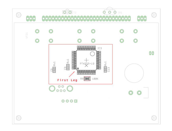
Step 6: VFD drive Chip
Flip the PCB to the other side then we can solder the components on this side. The major chip on this side is PT6315 VFD Chip in LQFP-44 package; Use the same skill of soldering the MCU to solder this chip. Also please double check the chips' pins carefully after soldering.(* Please note that the PT6315 chip may have two round hole marks on its surface, the small hole marks the first leg.)
Please solder the 3PCS 0u1F capacitors and 100K resistor (* key component, do not change the value) too.
Step 7: First Testing
After finished all the 6 steps shown up, now we can plug the VFD48 panel in the PCB(Do not solder it!) and plug the USB power in, use hand to push the panel a little bit up to make sure all the legs touched the pad; If all fine the clock will started displaying and ticking, please check all the segments inside the panel to see if can be light up correctly. If some segments do not light up, please check if some legs of the panel did not contact the pad correctly or tightly or some legs of the PT6315 chip did not be soldered correctly. If the two or more segments are lighted up together, may have the short among the PT6315 legs.
If all fine, unplug the panel we can do the next step.
Step 8: Cleaning Circuit Board
You can use the household rubbing alcohol and a toothbrush to remove the solder flux on the PCB. If available, the anhydrous alcohol (used for electronics cleaning) works much faster. Blot the cleaned area with a non-linting tissue (like Kimwipes EX-L) or a clean towel or you can do it in your own way.
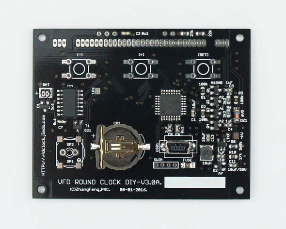

Step 9: Buzzer part
Buzzer Part is easy, first solder the [G21] Digital Transistor (Note: If damaged this component, you can replace it with the SI2302[A2SHB] N-MOSFET);Then Solder the buzzer part, we have two types of the buzzer, one is the SMD Version, the other is the DIP version, please solder the one which you find in the KIT.
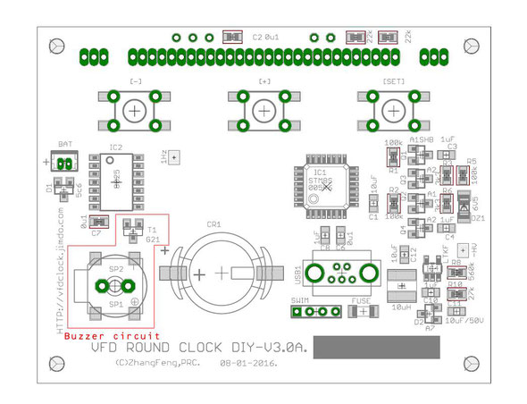
Step 10: Buttons part
There are 3PCS of the buttons on the PCB, usually you will find 3PCS 6*6 SMD version of the buttons in the KIT. If you have enough soldering skills, you can solder those buttons directly or we recommend that you use long flat nose pliers to band the button legs straight, then you can plug the buttons inside the PCB holes, and then solder the legs.
Step 11: Test the buttons, buzzer, and VFD panel
After finished all the steps shown up, we have almost finished assembling the PCB. At this time, we recommend plug the USB power in, then click the button(s) to see if all the button(s) in working, and to see if the buzzer can beep when you click the button.
If all fine, you can unplug the USB power, then plug the VFD48 PANEL in the PCB holes, then plug the USB power back to give it a light up test.
We suggest that you use your hand to push the vfd48 panel a little bit up to make sure all the VFD panel legs touch the PCB holes, if all fine, the VFD48 panel can be light up and will start to display the time, please wait for at least one minute to check all the segments inside the panel to make sure all can be light up properly.
Step 12: Solder the VFD48 Panel
When soldering the VFD48 panel, we used to solder the left and right two legs first, then adjust the high of the legs(by using the solder) to make sure the panel has the same height at the both sides. Then you can use sharp scissors to cut all the legs short and solder all the legs (Because of the legs are really close, please be patient and do it carefully).
After finished assembling the PCB, you can do the test again.
Then you can clean the buzzer and the buttons and panel legs by using the cotton swab with alcohol (or other things you have).
Notice:
Please do now wash the Buzzer/Buttons by alcohol or will be damaged!
Please do not wash the VFD48 Panel in the ultrasonic wave cleaner, may damaged the filament!
If necessary, you can add a small size (like 0.5cm*1.5cm) 3M double stick foam tape to glue the panel on the PCB.
Step 12: Solder the Extras:
If have IR function, you need to solder a IR receiver on the front side. We recommend you band the IR receiver legs in 90 degrees (aware the direction), then plug it inside the PCB holes then solder it. Because of the IR receiver is heat sensitive equipment, please control the temperature and solder it fast.

Write a comment