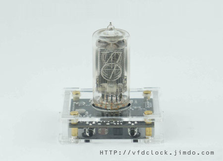
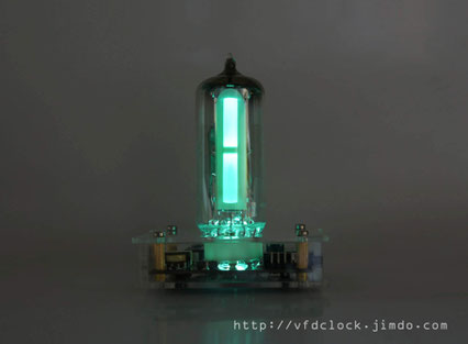
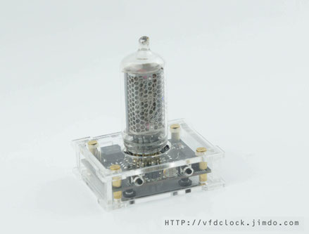
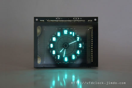
 NIXIE CLOCK DIY
Tue
30
May
2023
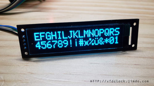
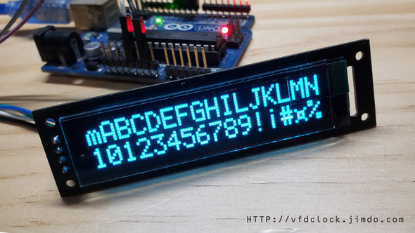
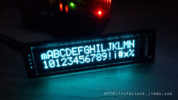
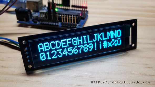
3V3~5V 3.12# OLED 256x64 16-level grayscale module SPI/I2C for Arduino

Sun
19
Feb
2023
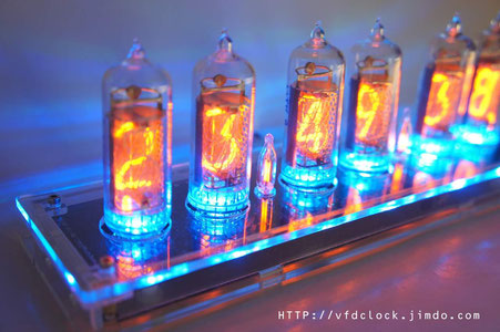
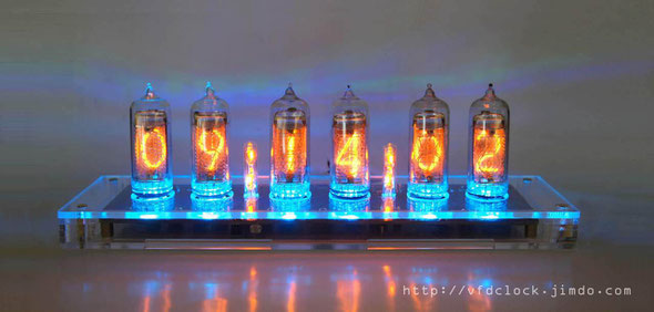
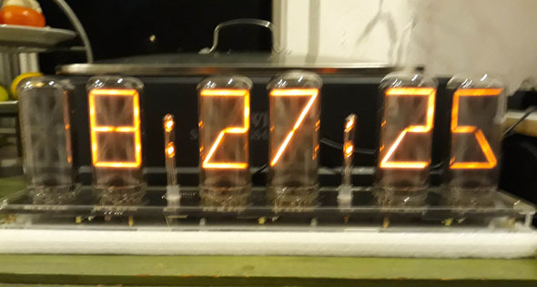
USB powered,IN18 6-tube Clock DIP40 KIT
5V USB Powered-IN-18 6-tube Clock DIY version (DIP40)
Assembly Instructions
V1.0

Tue
11
Jun
2019
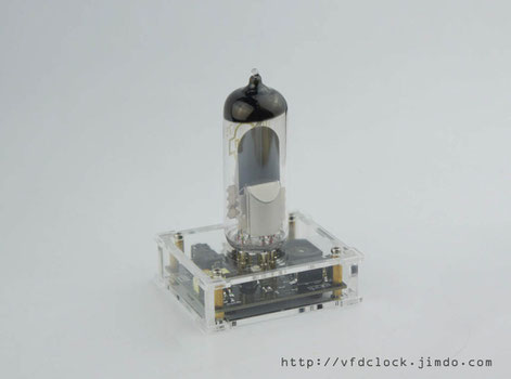
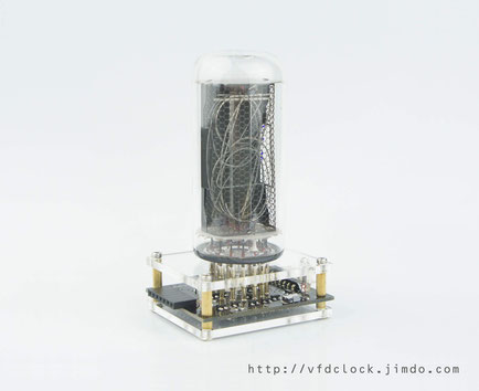
USB Powered 6E1P(EM80) 2-tube Magic Eye VU Meter(Stereo Audio Visualizer)-V1.0
Sat
04
May
2019
DIY KIT-5V USB Power-Pluggable IN-18 6-tube NIXIE clock-Assembly Instructions
Sat
10
Feb
2018
DIY DIP KIT-Pluggable IN-18 6-tube NIXIE clock-Open Hardware
Sat
12
Nov
2016
New-[HV12-Pro]-12W-Small Size-12V to 380V(Max) High Efficiency PSU for Audio Application
Sat
17
Sep
2016
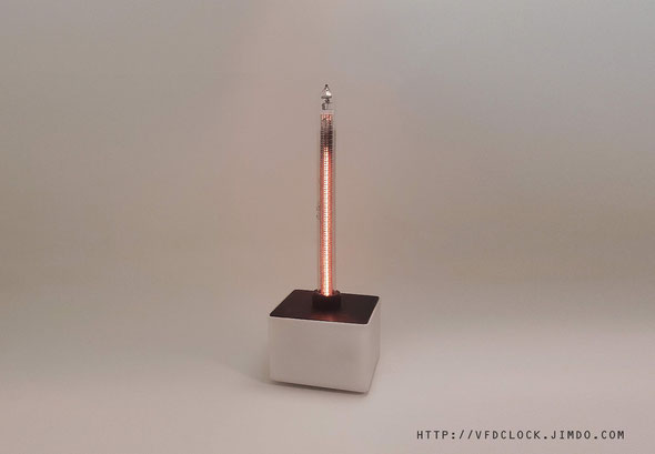
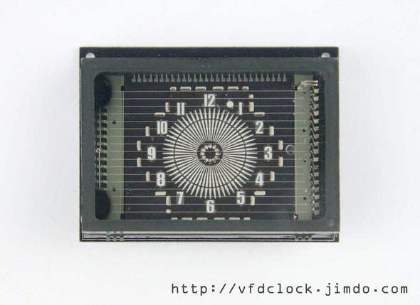
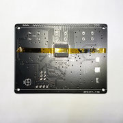
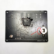
USB Powered VFD48 Analog-style Unique Round VFD Clock Assembly Instructions

Wed
31
Aug
2016
New-USB powered-IN-18 6-tube NIXIE clock with glass tube middle dots
Sat
20
Aug
2016
New-Plug-able IN-14 6-tube NIXIE clock with glass tube middle dots and with AC driving circuit

Tue
26
Jul
2016
Plug-able USB Powered-Li-poly battery drive-able ,Two-Digit IN-18 NIXIE Tube Clock-Pro.

Sun
24
Apr
2016
Plug-able USB Powered-Li-poly battery drive-able ,Two-Digit IN-14 NIXIE Tube Clock-Pro.

Mon
02
Nov
2015
Z586M Huge Single Digit NIXIE Tube Clock-Pluggable-USB Powered

Fri
23
Oct
2015
433M Wireless GPS Time Station for NIXIE clocks (OLED Version)-V1.0

Sun
26
Jul
2015
OpenHardware-Pluggable-USB Powered IV-11 Single Digit VFD Tube Clock
Sat
18
Jul
2015
Open Hardware-Highly Optimized-10W-MC34063 based High Voltage power supply module-High efficiency up to 85%-Small Size
Wed
01
Jul
2015
New-HV12W PSU,5V~12V DC in,170V DC out,designed for driving 6-tube IN-18 NIXIE clock-92.6%(Max) high efficiency

Thu
04
Jun
2015
10W-120kHz High Voltage Supply Module-Designed for Audio Amplify Circuit

Mon
25
May
2015
Open Hardware-MC34063 based High Voltage Power Supply Module-10W

Fri
08
May
2015
Open Hardware - GPS Receiver Module for NIXIE/VFD clocks
Sat
07
Mar
2015
NEW-Plug&Play IN-14 6-tube NIXIE Clock V1.2
Tue
10
Feb
2015
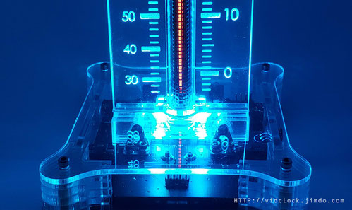
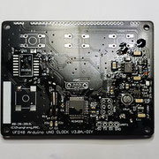
VFD48 Round VFD Module For ARDUINO/51/AVR/STM8S/STM32 etc.
Tue
27
Jan
2015
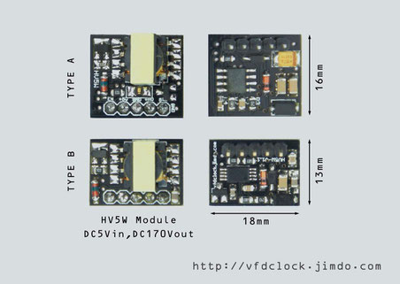
New-HV5W NIXIE High Voltage Module,5V DC in,170V DC out
Fri
16
Jan
2015
Pluggable - USB Powered IN-14 SD NIXIE Tube Clock+Hard Legs Tube.
Thu
15
Jan
2015
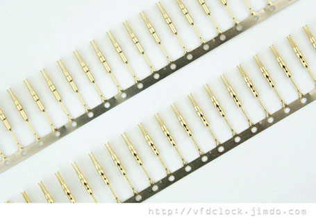
Customized the NIXIE PINS from the factory,1U gold plated,Very high quality
Tue
28
Oct
2014
USB Powered 6E1P(EM80) Magic Eye VU Meter(Audio Visualizer)-V1.0
Sat
23
Aug
2014
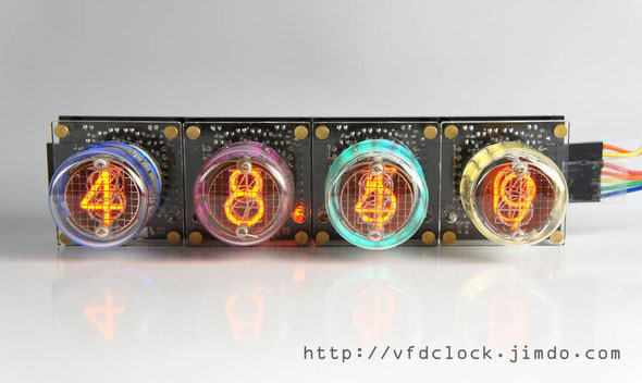
USB Powered 6-Tube IN-14 NIXIE clock V1.0-USB供电的IN-14辉光管时钟
Sun
17
Aug
2014
IN-18 Nixie Module for ARDUINO 为ARDUINO设计的IN-18辉光模块
Sun
17
Aug
2014
New-HV15W High Voltage NIXIE and Magic Eye Tubes PSU,Power Supply Module V1.0 Std.-MAX1771 Version

Tue
22
Jul
2014
BOE VFD48圆盘时钟正式版-USB Powered BOE VFD48 Analog-style Unique Round VFD Clock With Enclosure
Sun
20
Jul
2014
Very Rare NEC CD66-A Single Digit NIXIE Clock V1.0-
Sat
19
Jul
2014
USB供电的单管6E2猫眼音量指示器-USB Powered 6E2(EM84) Magic Eye VU Meter(Audio Visualizer)-V1.0
Sat
19
Jul
2014
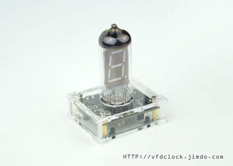
IN-8 and IN-8-2 Single Digit NIXIE Clock V1.0
Sun
15
Jun
2014
BOE圆盘荧光钟-USB Powered VFD48 Analog-style Unique Round VFD Clock
Sat
10
May
2014
IN-14单管辉光时钟-1.1版-USB Powered IN-14 Single Digit NIXIE Clock V.1.1.
Mon
05
May
2014
IN-18 Single Digit NIXIE Clock
Mon
05
May
2014
QS27-1 单管辉光时钟 V1.0 QS27-1 Single Digit NIXIE Clock


Wed
02
Apr
2014
IV-11 单管VFD时钟 IV-11 Single Digit VFD CLock V1.0

Wed
02
Apr
2014
IN-12A/B 单管辉光时钟,IN-12A/B Single Digit NIXIE Clock V1.0

Wed
05
Mar
2014
为ARDUINO设计的QS30-1辉光管模块 QS30-1 NIXIE tube module for ARDUINO v1.0
Sat
01
Mar
2014
QS30-1单管时钟-1.0版-QS30-1 Single Digit NIXIE Clock Ver.1.0.

Thu
20
Feb
2014
IN-14单管时钟-1.0版-IN-14 Single Digit NIXIE Clock Ver.1.0.
Wed
08
May
2024
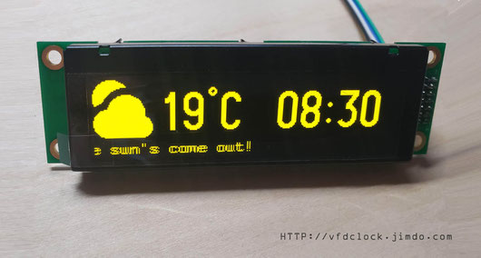
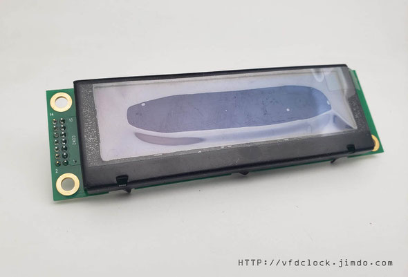
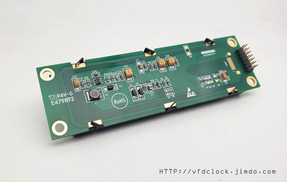
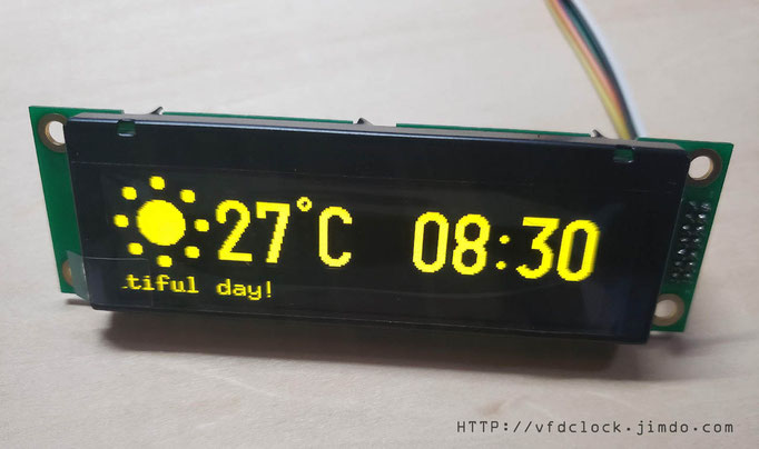
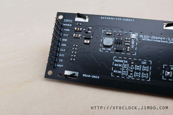
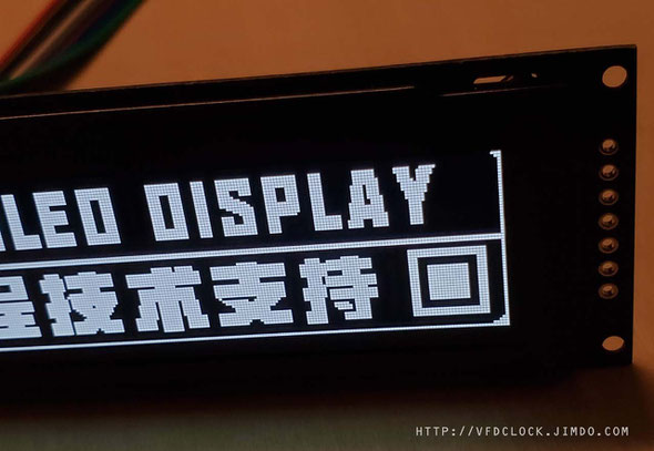
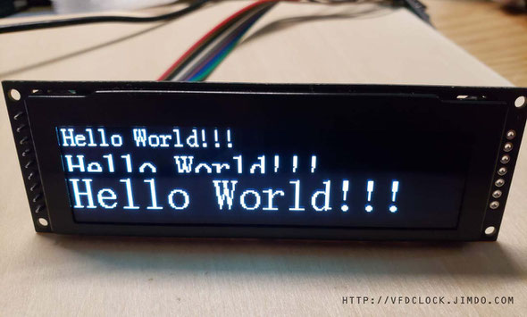
HGS256642 3.12# YELLOW OLED display module

Features:(For reference only)
HGS256642 3.12# YELLOW OLED display module
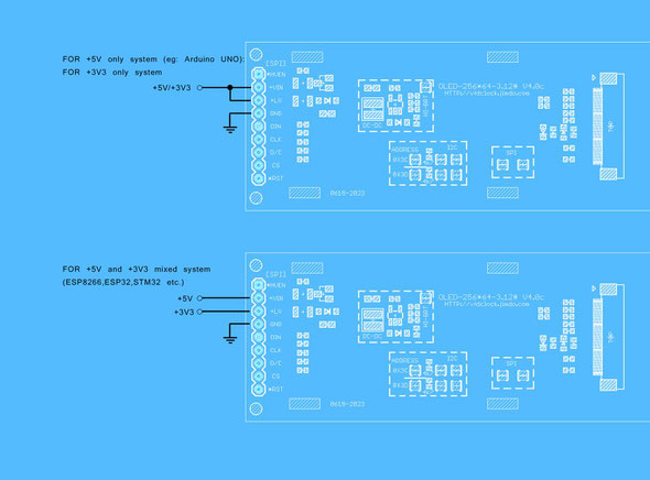
Main Power:+3V3 only(Do not use 5V!!!)
Logic level:+2V8~+3V3
Current:~280mA
Driver IC:SSD1322
Module Size:105.6mm(L)x31.8mm(W)x9.5mm(H) (MAX.)
Visible Area: 78.78mm(L)x21.18mm(W)
Res:256*64
Color:Yellow
MCU Interface:
(Interface can be changed by soldering the 0R resistor on the back of PCB):
8-bit 8080(In default)
8-bit 6800
4Wire SPI
3Wire SPI
CON:14pin(2mm gap)
ARDUINO U8G2 lib can driver it directly,have tested om ESP8266 and ESP32-C3 platform via SPI 4-wire mode;
In editing..................


Wed
08
May
2024
HGS256642 3.12# YELLOW OLED display module
Features:(For reference only)
HGS256642 3.12# YELLOW OLED display module
Main Power:+3V3 only(Do not use 5V!!!)
Logic level:+2V8~+3V3
Current:~280mA
Driver IC:SSD1322
Module Size:105.6mm(L)x31.8mm(W)x9.5mm(H) (MAX.)
Visible Area: 78.78mm(L)x21.18mm(W)
Res:256*64
Color:Yellow
MCU Interface:
(Interface can be changed by soldering the 0R resistor on the back of PCB):
8-bit 8080(In default)
8-bit 6800
4Wire SPI
3Wire SPI
CON:14pin(2mm gap)
ARDUINO U8G2 lib can driver it directly,have tested om ESP8266 and ESP32-C3 platform via SPI 4-wire mode;
In editing..................
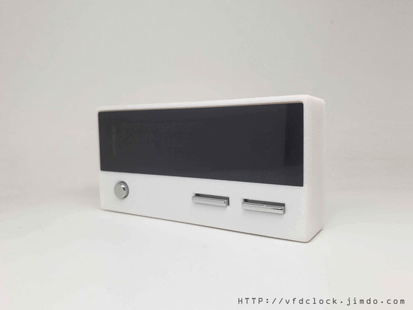
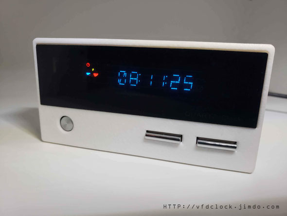
Mon
08
Apr
2024
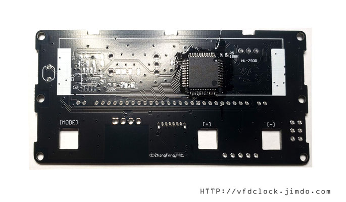
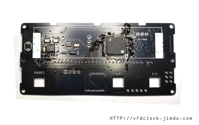
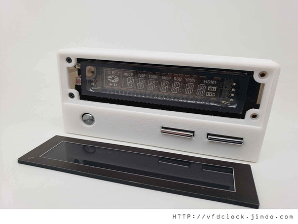
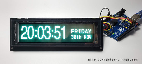
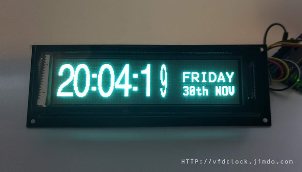
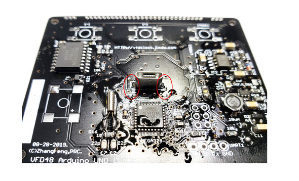
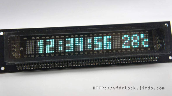
5V USB powered Open Source Arduino VFD clock Assembly Instructions

1. It is recommended to start the welding work from the front first. The first part to be welded is the PT6513 driver IC. Use tape to temporarily fix the IC on the PCB and align the pins of the
IC. Please pay special attention to the direction of the first pin and do not mess with it. wrong;
Then apply flux on the pins and use a soldering iron to solder; use a magnifying glass to inspect after the soldering is completed to ensure that the pins are soldered correctly and there are no
false soldering or short circuits;
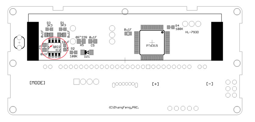
2. Solder the LM9022/AP9022 integrated circuit using the same method, also paying attention to the direction of the IC;


3. When welding the resistors, capacitors, diodes and other parts on the front, please pay attention to the correct placement direction of the diodes;

4. Turn the PCB over to the reverse side and use the same technique to solder the MCU Mega328 and RTC RX8025T, as well as other RCL and other parts; C23 and D4 on the lower left side are optional parts and are only used for the online UART programming port. If not needed Modify the program without welding;

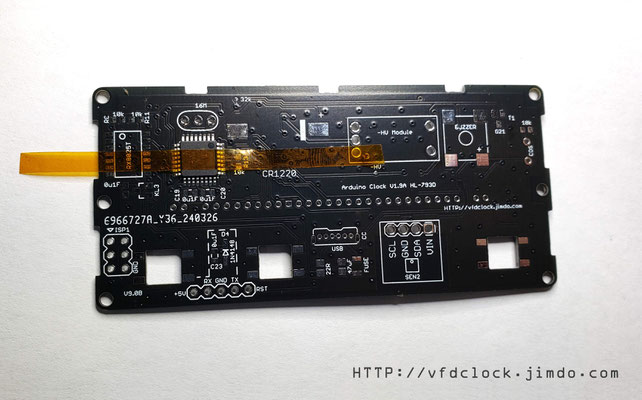


5. Then solder the female pin part used by the HV power module. First insert the female pin into the PCB, then cover it with a hard board, you can use PCB or wood chips, use clips on both sides to clamp the PCB, then flip the PCB over and solder the lower part;


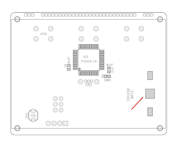
6. Weld the 16M crystal (the pins have no directionality), CR1220 battery holder (please pay attention to the installation direction) and CDS photosensitive sensor (it is recommended that the installation height does not exceed the height of the VFD screen);

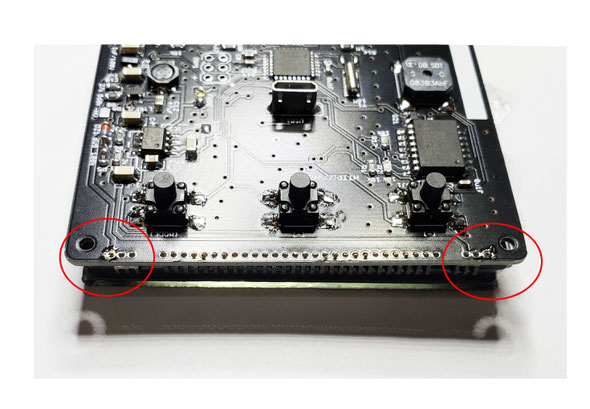
7. Solder the USB socket. First, insert the USB socket into the PCB. There is only one direction for insertion (as shown in the picture). Then flip the PCB and solder the left and right mounting pins first. After confirming that the USB position is correct and the installation is not skewed, you can solder the other ones. Pin; after the soldering is completed, flip the PCB over and add solder to the left and right lower sides of the USB socket to make it secure;


8. After the above welding work is completed, you can use alcohol and other cleaning agents to clean the PCB; because the RTC contains crystals, ultrasonic cleaning machines are not allowed!
9. Then weld the buttons and other parts. First, unfold the four legs of the button, flatten them with a tool, cut them short, and then insert them into the PCB mounting holes for soldering. The buttons have two specifications, the taller one is used for the [mode] button, and the two shorter ones are used for the [+] and [-] buttons; after the button welding is completed, the speaker can be welded (please pay attention to the "+" pin direction). After completion, the -HV power module can be inserted;
10. Install VFD screen. Before installing the screen, please confirm that the circuit board is working correctly. First insert the VFD screen into the circuit board, then apply force on one side to press the pins against the inner wall of the installation hole, and then plug it in for testing. If the VFD screen lights up correctly and displays normally , the pins can be soldered, otherwise the PCB fault needs to be eliminated before proceeding to the next step. When welding, make sure the screen pins are pressed as low as possible and as close to the PCB as possible (as shown in the picture), otherwise it may not be installed into the housing later;


12. Additional functions: If the clock is equipped with a temperature and humidity display function, you need to weld an installation socket for the temperature and humidity sensor, and directly weld the 5pin female socket to the corresponding position.
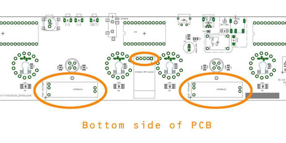
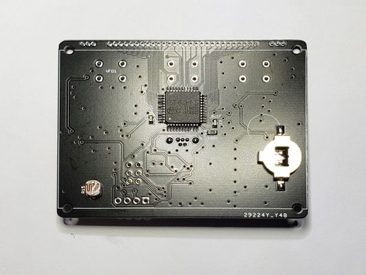
Top and Bottom sides of PCB

Enclosure assembly instructions
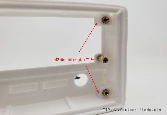
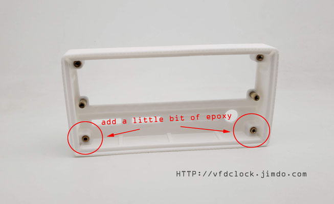
1. First install 6 M2*6mm (length) copper pillars inside the casing. The bottom two need to be bonded into the mounting holes with a small amount of epoxy resin. The remaining four are used on
the front panel of the casing. Screws for fixation;


2. Install the key cap on the key, press the key head firmly (please pay special attention to using your fingers or other things to support the bottom of the key when pressing to prevent it from falling off the PCB), and adjust the approximate position of the key cap. Then tilt the PCB into the case until it is in place. Please pay special attention to the fact that the key cap needs to be exposed from the front mounting hole; (Tip: If necessary, consider using a small amount of epoxy resin on the back of the PCB to stick the keys to the PCB. Prevent the button from detaching from the PCB due to excessive pressing force that may occur during use);

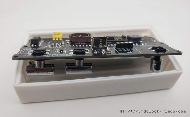

3. We recommend first using foam double-sided tape to stick the VFD screen to the PCB, then put the circuit board into the housing and place it in a good position, and then install the fixing copper pillars (M2*5mm ( Body length) + 3mm (screw length)) and screws. It is recommended to use tweezers to clamp the inner hole of the copper pillar for rotational installation;

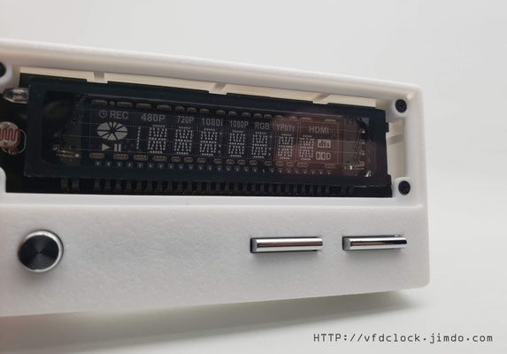
4. Install the front panel. First remove the protective film on the front panel. The protective film may have multiple layers. The last protective film on the front can be left until the final installation is completed and then removed. Use double-sided tape to install the front panel in place. Depending on the version Different, the front panel may have up and down installation directions, please pay attention;


5. The last step is to install the back panel. This part is relatively simple. You only need to remove the protective film of the back panel and then use screws to fix it in place;


6.Here is the final fully assembled VFD clock.

User Application Instructions
In editing...
Wed
17
Jan
2024
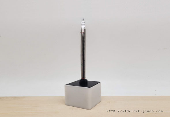
Open Source-DIP-USB Powered-Arduino NIXIE Thermometer-V2.0

This is the 2.0 version of 3 tube NIXIE thermometer, in this version,we move the USB socket to the middle back of the PCB,and added an 3.5mm female socket and a button(to turn the LED ON/OFF).
The oC and oF version use the same source code by adding an C/F jumper on PCB.
(Short the [F] jumper to select the oF version,left it open to select the oC version.)


Solder the female through hole pins first.
1. plug the pins on the TOP side of PCB;
2. cover a PCB or hard board on the top of PINS and hole it on PCB by using foldback clip;
3.Flip the PCB then solder the female pins;
In this version,we added 2 middle female pins to install LEDs, you can replace the LEDs by yourself by hand.
We add orange color LEDs we customized from factory in default, its colors are very close to NIXIE color. If you wanna another colors of LED,you can replace it by yourself. Most of the std. 3mm and 5mm dia. round LEDs all fit with the socket.
Solder the rest of the equipment on PCB as shown on the pic.
Aware the IC socket directions and remember to solder the VIN and HVout 2 jumpers.
In this new version,we add a jumper on the right-bottom of the PCB with MARK [F],if wanna display temperature in oC, left this jump open,if need to display in oF version,please short this jumper.
Do not solder the HV cap and transformer and 3.5mm audio socket and button,those equipment can not be washed.


The 2 pics be shown up are the PCB been washed. You can zoom the pics to compare with your PCB to see if all the equipment are be installed correctly.
When done, wash the PCB and make it dry.

When PCB be washed and dried,you can solder the transformer and button,.
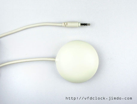
for the DS18B20 Part,you can solder it on PCB directly,and if you wanna install it in a 3.5mm audio jack ,you can solder a 3.5mm audio audio socket on PCB.

For how to create a DS18B20 sensor in a 3.5mm audio jack,please visit:
Create a DS18B20 sensor in a 3.5mm audio jack
Plug the LED on the top side of the PCB.
For LED part,recommend cut the legs short first,and aware the LED [+]leg and [-] leg.

Then plug the nixie tubes in the socket.
For oC version,you need to prepare:
2pcs IN14+1pcs [IN19A ИН-19A] NIXIE tubes;
For oF version ,you need to prepare:
2pcs IN14+1pcs [IN19B ИН-19Б] NIXIE tubes;
When done,Plug 3.5mm audio jack DS18B20 Sensor in the socket, then plug USB power, if all fine,the NIXIE tubes will display the temperature data after ~2 seconds.
Assemble the Acrylic enclosure
In editing.............
Wed
17
Jan
2024
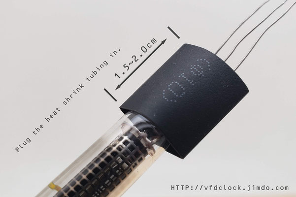
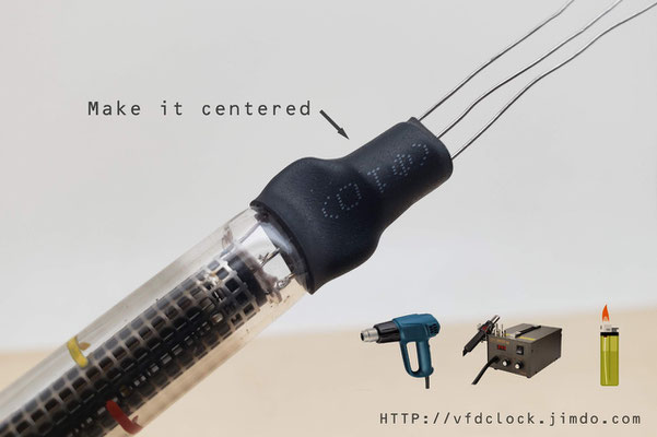
Create a DS18B20 Digital Temperature Sensor with 3.5mm Audio Jack

Hold the DS18B20 Digital Temperature Sensor with the 3.5mm Audio Jack Sleeve as the direction showed on the pic.
The circuit connection shows on the up pic,the 4k7~10k pull up resistor is optional.
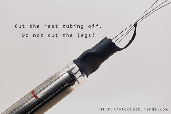
Band the first leg of DS18b20 up to the sleeve as GND pin.

band the middle pin and plug it to the middle pad of audio jack.

Cut the third pin short and plug it to the short&middle hole of the audio jack.

Solder all 3 pins like as shown on the pic.

Pull up resistor is optional,if need,u can solder an 4k7~10k resisitor between VCC pin and DATA pin.
Plug the PVC tube on.

Done!
Tue
09
Jan
2024
Open Source Arduino VFD Clock With ABS-Like Enclosure

A New design of VFD clock with ABS-Like enclosure.
in editing...
Assembly Instructions
You need to have ability to soldering the SMD equipment to do assemble this DIY KIT.
We use ...


Enclosure Assembly instructions
in editing...

Wed
20
Dec
2023
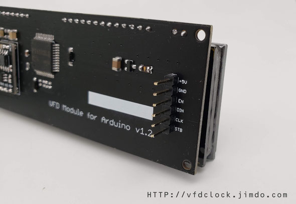
5V Ready-HL-D022 VFD Module for Arduino/Stm8/Stm32 etc.

This is VFD display module only,you need to do the audio circuit part by yourself.
HLD022.ino
Source code for driving the HLD022 VFD module.
Arudino 1.0.4
#define DIN_PIN 13
#define CLK_PIN 12
#define STB_PIN 11
Please use Acrobat Reader from ADOBE to open this PDF file and save the code.zip.txt file from attach part then rename it back to code.zip,decompress it by winzip,7Zip,winrar etc.
Please use Adobe Acrobat Reader to open it,you can find the source code zip file in the attach part of PDF.
Mon
09
Oct
2023
5V Ready-Futaba FUTABA-7-bt-317NK VFD display module

5V ready -FUTABA-7-bt-317NK VFD display module for Arduino;
Please note:
The first grid of a dot matrix can display few defined icons only, it is not a common dot matrix!
Compiled under ARDUINO V1.0.4 in pure C code.
Please use ACROBAT reader from Adobe to open the PDF file and find Source code files in attachments part of PDF.
You can find the password of PDF inside the parcel.
In editing.....
Specifications(For reference only)
VIN:5VDC/~150mA
Panel size: mm* mm
PCB size: mm* mm
Color: Green+ orange
Driver Chip: PT6315
Features:
1). 5V Ready, easy to be used. Can connect to your ARDUINO UNO board with only 3 signal wires;;
2). High efficiency power circuit, no transformer, no heat, Low HV, very safe, High Brightness;
3). All SMT components, very thin PCB, easy to be drived;
4). Contains over-current protection, and reverse
connection protection circuits;
5). Open source code for ARDUINO NUO, pure C code.
6). Simple 3-wire SPI interface, with EN pin, support shutdown the High Voltage and Filament Supply completely.
Interface:
3-wire SPI:
DIN
CLK
LATCH(CS)
--------------------
+5V
GND
EN - HV supply enable(optional)
For Video:
https://youtu.be/...

Tue
30
May
2023
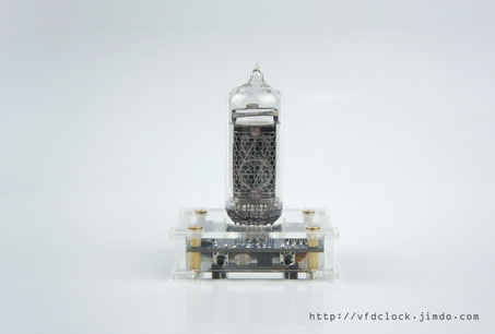
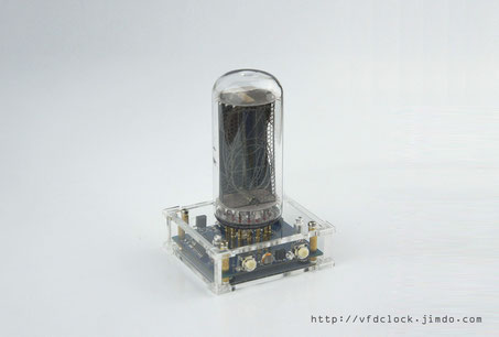
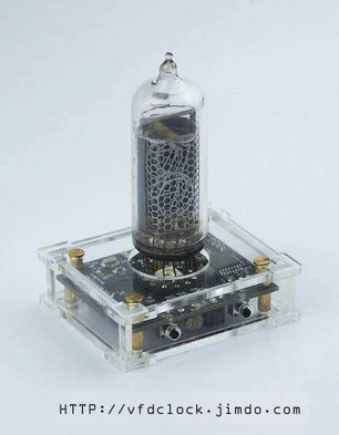
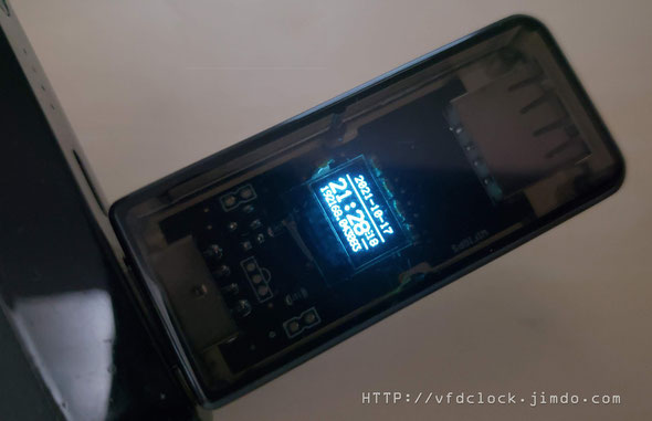
3V3~5V 3.12# OLED 256x64 16-level grayscale module SPI/I2C for Arduino
in editing.....
Because of the source code is too big to upload here,for customers who bought the module ,would please send us an email,we will send you the source code.
Please send to: zjjszhangf[at]gmail.com


Tue
21
Feb
2023
3).USB Powered,IN13 VU Display
In editing...


Install IN13 tube
test
test3
test4
test5

Tue
21
Feb
2023
2).USB Powered-PL14 NIXIE VU Display

PL-14 nixie vu meter,in editing....
more info will coming soon
add some text here...


How to install PL14 tube to main body by yourself.
test

test2
Mon
20
Feb
2023
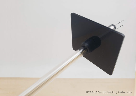
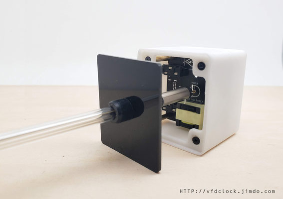
1). Overview :Our VU system
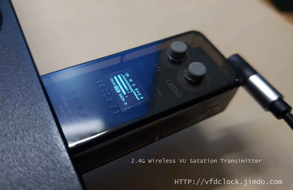


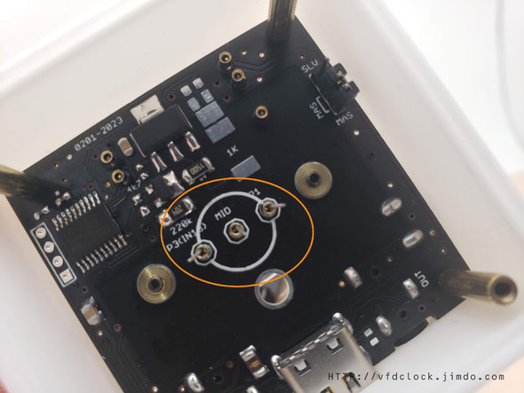
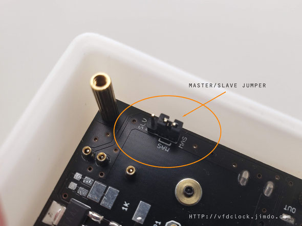
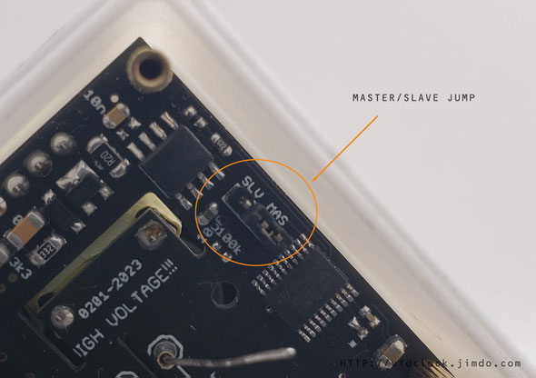
This is stereo VU system,it contain 2 main bodies be connected together by using a 3.5mm audio cable(do not plug audio signal directly via this socket).and set each internal jumper,by shorting the (MASTER) side of jumper,it will display Left channel VU data in default,if short (SLAVE) jumper,it will display Right channel VU data.
tips:The receiver contains swap L-R data button.
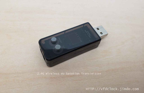
There are two 3.5mm audio sockets on the bottom side of Sender,they are same and be connected in parallel,use one to input the audio signal from like cellphone,desket computer,notebook,DVD player,mp3 player,etc.
and use the other one for earphone.
Would please do no connect the signal directly from speaker,may damaged chip inside Sender.

The sender contains 2pcs of buttons on the top,one is (mode) the other is (+).
In normal working mode,when u plug the USB power on,the sender will turn the OLED panel one,and display wireless channel first then display the VU meter of L(on top) and R(on bottom). All others info will be displayed on the bottom row.
You can change the signal gain by clicking the (+) button in -5~+5 range,and use (mode) button to change the smooth algothms in ORG(original signal),STD(standard 50% smooth),AGC1(gain fast,fade slow),AGC2(gain slow,fade fast),BAMBOO(50%smooth,min step set to 5).
How to set wireless channel?
USB power off first,then keep (+) butyon down no release,the plug USB power on,the OLED will display the set Channel info,then click (+) button to change the wireless channel,when done,click the (mode) button,the sender will make a test and save current channel info in flash,then reboot itself(may need 2~3 seconds).
The sender support CH01~CH12 total 12 different wireless channels. One channel signal can be receiver by multi receivers be set in same channel.

test
The receiver contains two buttons on the side,the front one is for setting the wireless channel from CH01~CH12,the top button on for setting the SWAP L-R (left-right) channel On/Off.
When L-R swap on the first Led digi segment will display (').
If receiver gets no wireless signal,the LED Segment display will be turned on,and displays the current channel and L-R swap state, when receives signal,the LED Seg Disp will be turned off.
It may have a small size of LED on the side ,it will go flash when received the signal.
Sun
19
Feb
2023
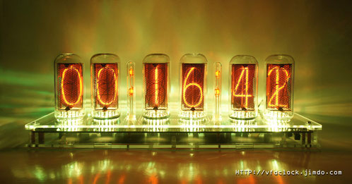
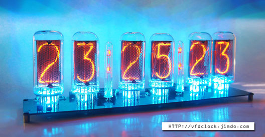
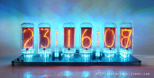
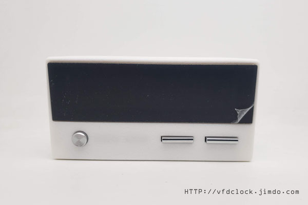
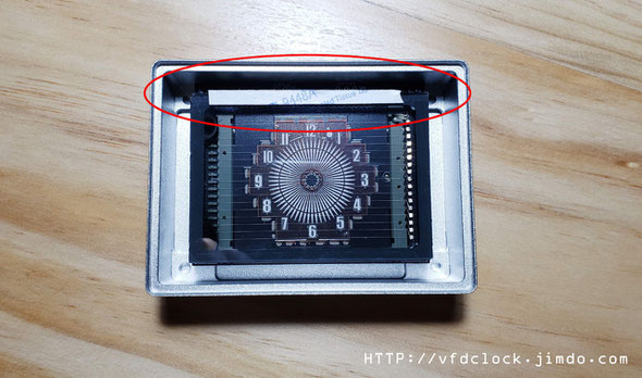
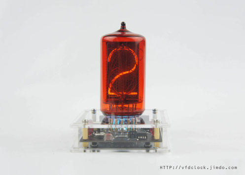
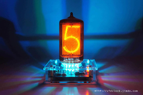
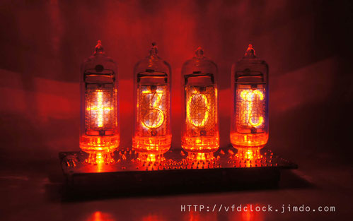
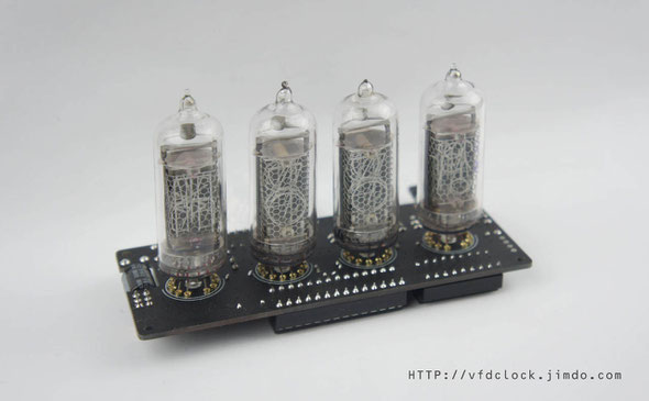
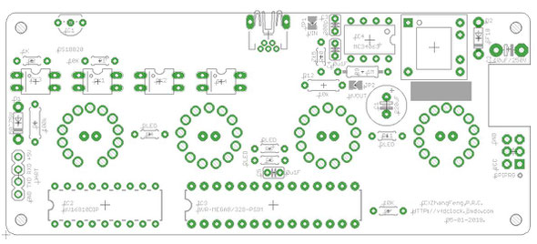
USB powered,IN18 6-tube Clock DIP40 KIT
5V USB Powered-IN-18 6-tube Clock DIY version (DIP40)
Assembly Instructions
V1.0
Notice:
For assembling this NIXIE KIT you need to have the skill of soldering DIP components.
We use a Hakko FX-888 Soldering Station (with CF2 Iron Head). We use 183℃(degree C)low melt temperature solder wire S60, 0.5mm(Dia.), Brand Almit.
And for most of the SMD components are big size and easy to be assembled,if you have a Hot air blower station,will help.
For how to solder the DIP components, we recommend:
https://www.hakko.com/english/tip_selection/type_bc_c.html
https://www.hakkousa.com/video/
Building it
Well, because of the circuit is block based and not very complicated, all you need to do is get all the components in the right position and make sure no short or no float before you plug the
power in. We will show the soldering steps blow.
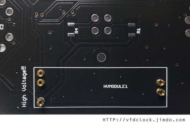
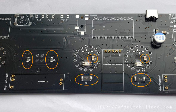
1): HV module Pins and WIFIGPS module PINS(Optional)
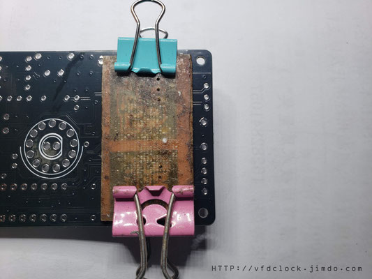
We need to solder some pins in this step,please solder it in this step,will be easier to be installed.
Please plug the Female PINs on the Bottom of the PCB then cover a had board like a small PCB or small
wood board etc.over the PINs, use two clamps to hold it with the main PCB, then flip the PCB. Now you can solder on the other side.
Tips: Because of the PINs are through hole version, please solder it carefully and do not let the tin goes in to the inside of the pins or will damage the PINs. If necessary, you can plug a
wood/bamboo toothpick in the bottom of PINs hole when soldering.


2): Solder the resistors and caps on the bottom side
The resistors are all in big side like 1206 or 2412,easy to be installed,and the caps for LED is in 1206 size.
For caps near LEDs,we recommend solder the caps first if you are using Hot air blower station,or the hot air may damage the LEDs.
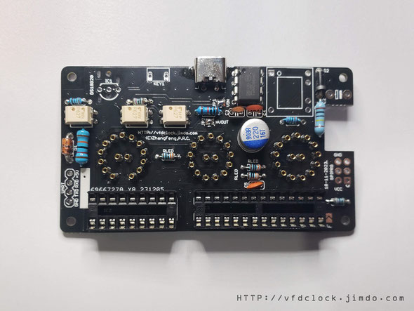
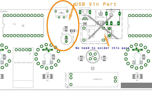
3): Install Main power and others components
The main power part has a USB socket(May in MINI USB/Micro USB/TYPE C,install only one USB socket),and a fuse, a 100nf cap and a Big Aluminum Electrolytic Capacitor(Please take care of it's direction).
No need to solder the 12V->5V buck convert part as shown on pic blow.(This part may not even exist in some of the PCBs, just Ignore it).

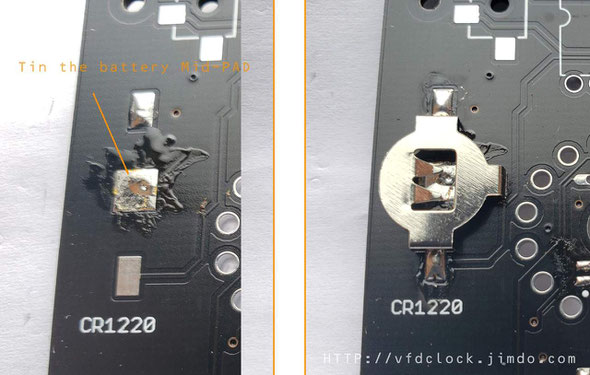
4): Install the CR1220 battery socket
In this part,we need to tin the middle battery pad first,then solder the metal holder,please do not add to much tin on the middle part.
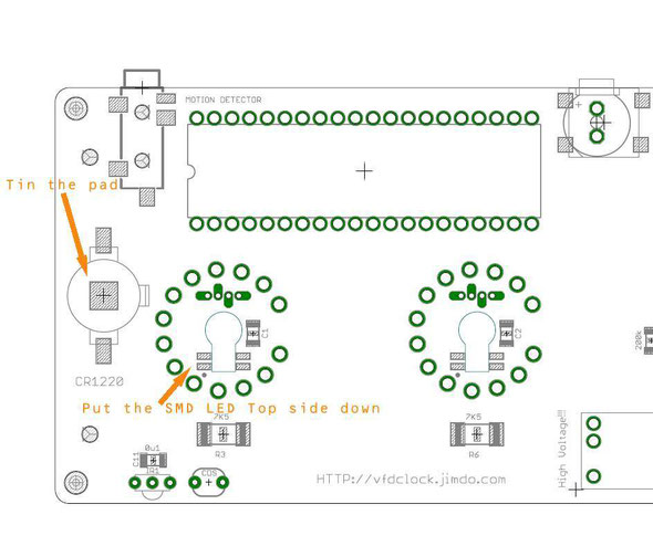
5): Solder all LEDS
May have two type of LEDS can be installed on PCB, one is smd version ,the other is dip version,would please install only one type of LEDS,do not install two types.
First ,we need to aware the first leg of LED,do not go wrong direction.
Second.LED is easy to be damaged when soldering,we need skills for low down its temperature.
For SMD version of LED,need to use a slim metal stuff to touch its soldering pad as a heat sink. We use a Solder paste scraper as heat sink,you can use utility knife instead if
you do not have one.
You can use tape to protect the IN-18 soldering holes on PCB when soldering the LEDs.


For soldering DIP version of LEDs,Use a bundle of copper wire to wrap around the pin a few rounds as
heat sink. Then plug the LED in the PCB and solder it,when done,remove the wire.


6): Solder all IC sockets
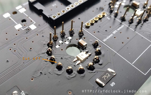
We need to install 3pcs of IC sockets,one is the main MCU module in DIP24 and the others are two DIP40 NIXIE driver module socket,please aware the direction of the sockets ,do not go invert.
We recommend u cut the thin legs of the socket before solder it on PCB as shown on the pics blow.


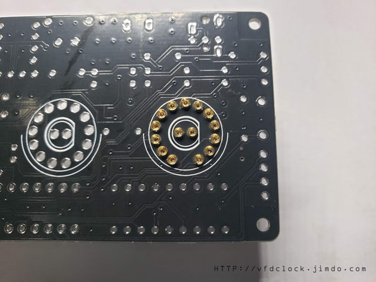
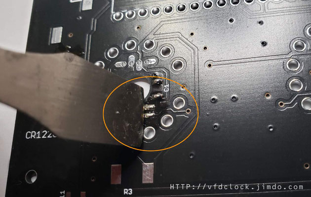
7): Solder Middle Colon Pins
The middle colon pins are on the top side of PCB,solder it a u solder the HV-module pins before.

8): IN-18 PINS
Now we are going to solder the IN-18 PINS.Please flip the PCB to the front side,the PINS need to be installed on this side and please solder it on the middle part of the PINs;
First we recommend you plug the PINS in the IN-18 legs,then plug ALL the PINS to the install holds,plug it down to the middle part, then flip the PCB ,solder the PINs on the bottom side of PCB;
!!!Plase double check to see if all PINs are plugged to the middle part before you solder the PINs!!!


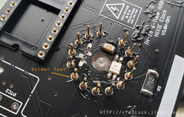
In soldering the PINS,if necessary,you need to keep pushing the tubes down to make sure all the PINS have been soldered on the middle part, please trade care of this part.
!!!Pleas note, do not add too much tin in soldering PINs,and please solder it fast. If add to much tin, the tin may go inside of the PINs and will solder the IN-18 tube legs with the socket,which will be big problem. We recommend add a little bit body lotion or oil on the surface of all in-18 PINs, will help to prevent be soldered together with socket.
Make A fast testing:
And after finished soldering on tube PINS,give it a power on test(*Remember to plug the MCU module and Driver Modules and HV mpdules in socket for testing) to see if have any problem.
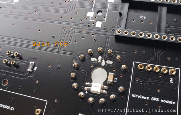
9): Cleaning the Circuit Board
You can use the household rubbing alcohol and a toothbrush to remove the solder flux on the PCB.
If available, the anhydrous alcohol (used for electronics cleaning) works much faster. Blot the cleaned area with a non-linting tissue (like Kimwipes EX-L) or a clean towel or you can do it in your own way.
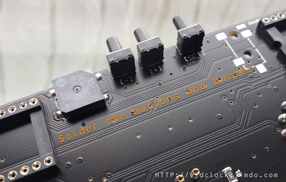
10): Buttons and Buzzer
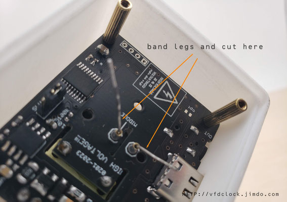
Because of Buttons and Buzzer etc. can not be washed, we need to solder 4pcs Keys and 1pcs Buzzer after cleaning the PCB. If the Buttons are one side two pins version,just solder it directly on PCB,if the Buttons are two side 4pins version,cut one side 2 pins off buy yourself,and band it flat the other side of 2pins then solder it and cut it short(or cut it short first before soldering);
Extras :
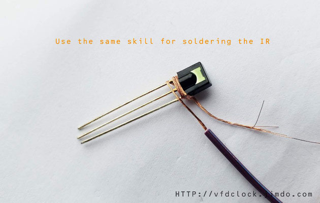
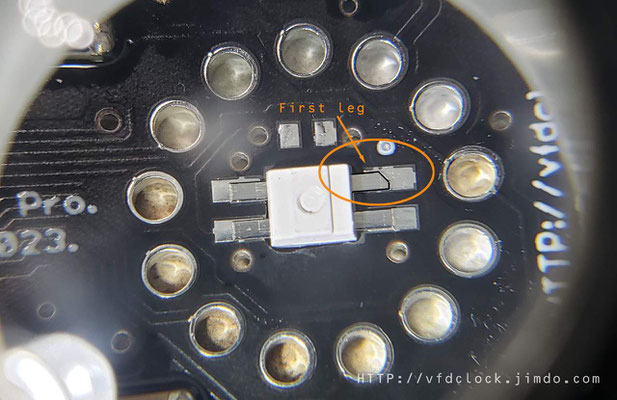
The IR function is optional,you need to solder the IR sensor on PCB,use the same skill of soldering the DIP LED as shown in the pic.
And is also have WIFIGPS module,you can just plug the module in the middle-front side(bottom) of PCB .
For how to setting the WIFIGPS, please check:
If it has UART BPS menu ,please select :9600bps.

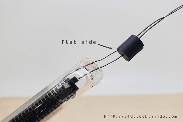
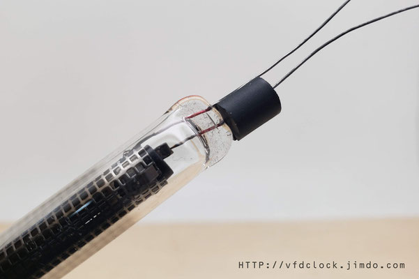
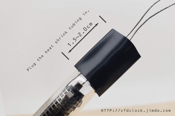
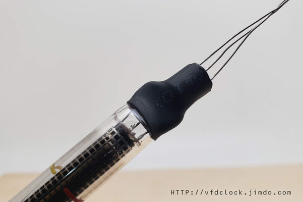
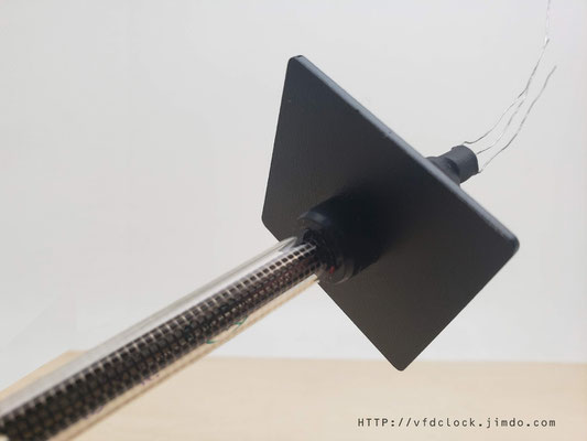
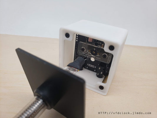
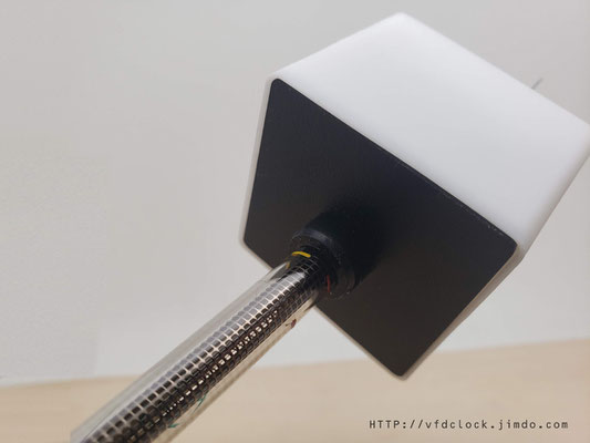
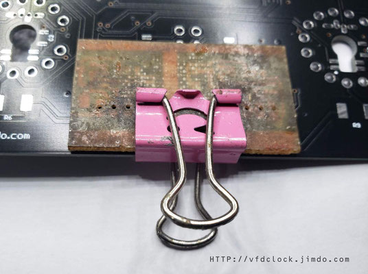
11): Create middle comma
For how to assembling the Middle comma,please visit:
KIT-Create the Middle Dot Comma for IN-18 NIXIE clock
You can make your own decision of the location of the bulbs in the middle glass tube.
The full map of the clock.


Sun
19
Feb
2023
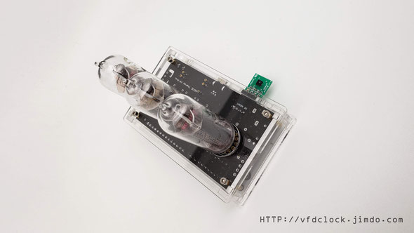
Open Source,3-tube Nixie Hygrothermograph DIY kit

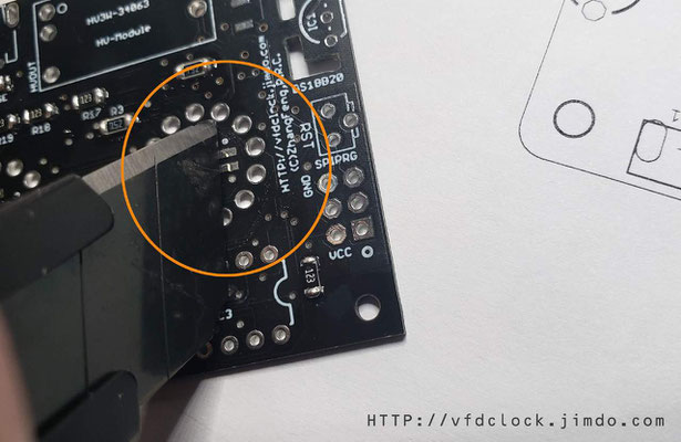

Solder the LED ,plug the LED on the bottom side of PCB,the lighting side face on the top of PCB,sware the first leg of LED as shown on Pic.
LEDs are heat sensitivity equipments, if possible, use 130C low temperature soldering wire,or use a slice metal(the pic shows back side of a paper knife blade) as heat sink,the solder the LEDs,and if possible,protect the nuxie holes by using kaptin tape.
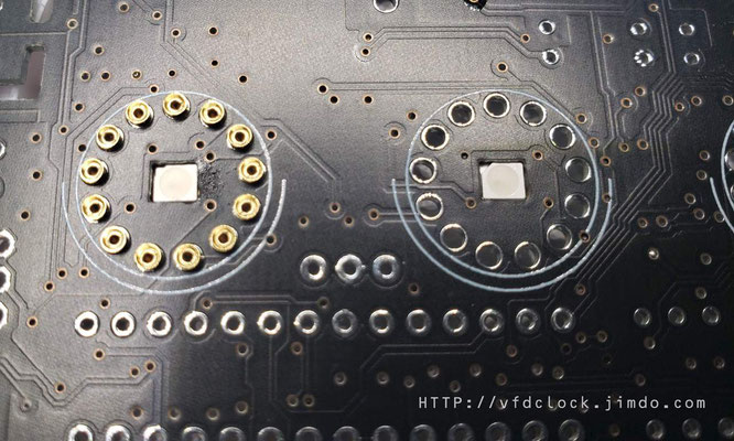
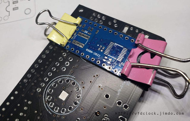
Solder the socked pins of Nixie tubes. First plug all female pins from the top side of PCB,then clip it on by using a small size PCB on the top with a clip.
Flip to the bottom and solder all pins on.
When done


Solder the HV module 5 pins female sockets.Same clip on skill.

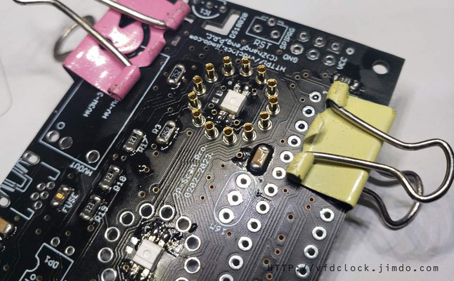
Solder the I²C 4-pin socket,big glass diode,16M resonaror(both mounting directions are all ok) and the USB socket.
Solder all the IC sockets,aware all the sockets direction.
Then wash the PCB to make it clean.
Solder the 3.5mm audio socket and button. These two equipments can not be washed.
Plug all the ICs and OP modules and HV3W DC-DC module and the sensor(face top).

Solder 4-pin male pins on the top of sensor module.
Tue
21
Dec
2021
5V Ready-VFD128*64 Dot Matrix Module for Arduino UNO

In editing...
VFD dot matrix 128*64 display module Features(For reference only)
1. 5V main power ready, 5V/3V3 IO part;
2. Support Arduino UNO , pure C source code;
3. Global brightness adjustable;
4. Module Based driver board;
5. Self protect scanning circuit with input inverse protection;
Size: mm;
Weight: g;
Power: 5V main power(5V/3v3 for GPIO);
Current: mA;


Fri
22
Oct
2021
USB-WIFIGPS OLED Version-Sync time with NTP server via WIFI

[For reference only]
In this guide you’ll learn how to config and use the WiFiGPS.
Plug WiFiGPS into USB power socket,if this is the your first time running the WiFiGPS, you need to do some configuration.
You can use a device that supports WIFI connection, like your computer, your laptop ,android cellphone etc.,Then scan for WIFI networks and you should see WIFIGPS-APxxxxx listed.
Connect to this WIFIGPS-APxxxxx WIFI hotspot, then using your web browser go to 192.168.4.1 and you should get the WifiGPSManger main page.(!!!If can not connect to 192.168.4.1,Would please check if you have set VPN or PROXY etc. in your web browser,if so,remove or turn those stuffs off!!!)

For the first time setup,recommend you enter the [Setup] part first,when click the [Setup] button,will list WIFIGPS NTP part parameters for you to set.
The [NTP SERVER NAME] part,you can set or select your own NTP server or select via the list(Please delete the server name first then click the right arrow,will show all predefined servers in the lists,recommend using pool.ntp.org).
Select your [Time Zone] via the second list. The first 7 lists are currently with auto Daylight support (in testing) shown blow.
AustraliaEst-Sydney(GMT+10:Daylight);
CentralEurope-Paris(GMT+01:Daylight);
UK-London,Belfast(GMT+00:Daylight);
US Eastern-NewYork(GMT-05:Daylight)";
US Central-Chicago(GMT-06:Daylight)";
US Mountain-Denver(GMT-07:Daylight)";
US Pacific-LA(GMT-08:Daylight)";
In the [User Define Time Offset(ms)] part,you can set time offset in like +500 for current time+0.5sec,or like -500 for current time -0.5sec to set the time offset you want.If no need this function,set it to 0.
The last [User Define Update interval(sec)] means how many time interval will WIFIGPS sync time via NTP server,like if set to 3600, the WIFIGPS will sync time online via every 1 hour.
(!!!Recommend set in no less than 60 sec. In some of version,if set to 0,the WIFIGPS will enter power save mode,in this mode,the WIFIGPS will do loop,like try to sync time online,then output time data for ~20 sec,then back to sleep for ~30 min,then wake up again!!!).
The [Show WIFI Advanced Options] if be selected,you can set like "Static IP address"... in [Configure WIFI] part.
When all set,click the [SAVE] button blow.

Then back to main page,enter [Configure WiFi] part,enter your WiFi SSID and Password in it,then click [SAVE] button blow.
usually after finished setting the WiFi SSID and Password,the WiFiGPS will reboot,if not,please re-plug the USB power to force it to reboot.
If all setting is correct,the WiFiGPS will try to connect to your WiFi hotspot then sync via online NTP server to get the current time,then output the time data via USB D+ pin in 5V 9600Bps UART output.
Sample Output Format:
$GPRMC,000000.000,N,0000.0000,N,00000.0000,E,0.0,0.0,000000,0.0,E,S*18
$GPRMC,000000.000,A,0000.0000,N,00000.0000,E,0.0,0.0,000000,0.0,E,S*XX
Output speed in 0.5sec per one $GPRMC string.

For the STD. version of WiFiGPS,it contains an led on PCB,when in configure mode or can not connect online or can not get NTP time data,the LED will be turned ON;
When everything is fine,it can SYNC time online and output time data,the LED will be turned OFF.
If you are using OLED version of WiFiGPS,more info will be displayed on the OLED screen on PCB.(If in Power Save mode,the OLED brightness will be turned OFF or in the lowest brightness for saving power).
Reconfigure or reset setting
If you have set the configuration already and you want to reset it,it may have a button on PCB for some version.When the WiFiGPS works in normal working mode(LED OFF,Time Data output in normal) then keep this button be clicked for about 4 sec,will reset all the configuration data.
If it contains no button or you do not wanna click the button,you can turn off your WiFi or move WiFiGPS to a far location where it can not receive the pre-defined WiFi signal,then plug the WiFiGPS in the USB power,wait for a while...,when WiFiGPS can not find pre-defined WiFi hotspot,it will enter the setup mode by itself.
Fri
22
Oct
2021
USB-WIFIGPS Std. Version-Sync time with NTP server via WIFI
Mon
23
Aug
2021
5V USB-ARDUINO NIXIE 3-Tube Thermometer+Humidity

In editing

Feature(For reference only):
1.Silicon based Temperature+Humidity sensor outside PCB via I2C(via 4pin socket on PCB, can ext out <20cm by urself if u want), high accurate, auto switch displaying the temperature and
humidity info on NIXIE tube;The first IN-14 left DOT will be light up if digits over 99 or less than 0;
2.5V USB powered and fully assembled PCB with acrylic enclosure and pluggable female pins on PCB,users only need to plug NIXIE tubes on it by hand;
3.Module based structure via socket,HV module can be replaced by hand, easy to replace it;
4.RGB LED under the NIXIE tube,u can switch the LED color by clicking the switch on PCB,item supports a few pre defined pure colors and rainbow color loop function;
5.ARDUINO UNO (ATMega328) fully open source pure C source code;
6.New NIXIE driver circuit, nixies display in high brightness;

Wed
26
May
2021
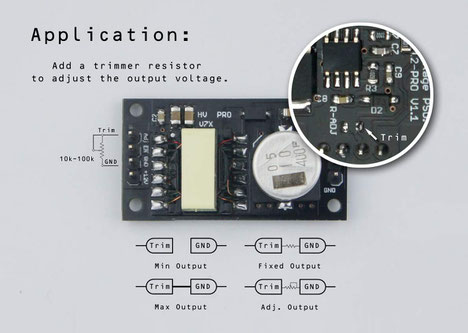
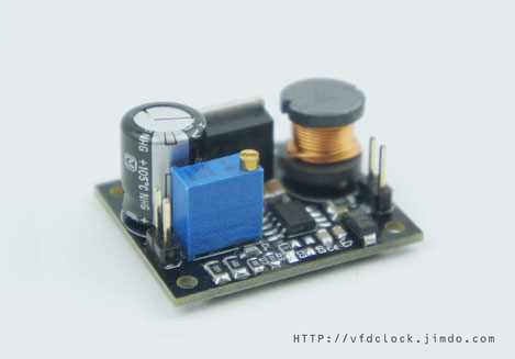
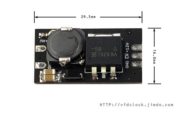
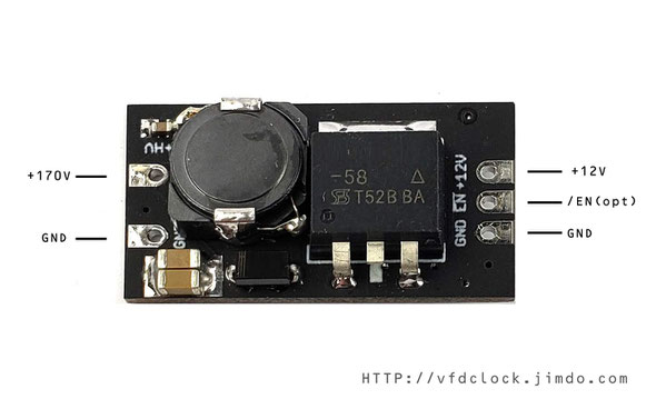
5V Ready-[HX3WE] High Voltage for Driving NIXIE tubes etc.

This is a small size module ,can light up 3~4 pcs if IN-14(or IN-12) nixie tubes with 15k
resistor in serial,or 2pcs in-18 big nixie tubes with 7k5 resisotor in serial.
We use this module for driving out 3-tube IN-14 NIXIE Thermometer,4-tube IN-14 NIXIE Thermomete,4tube DIY IN-12 NIXIE clock,all work fine.
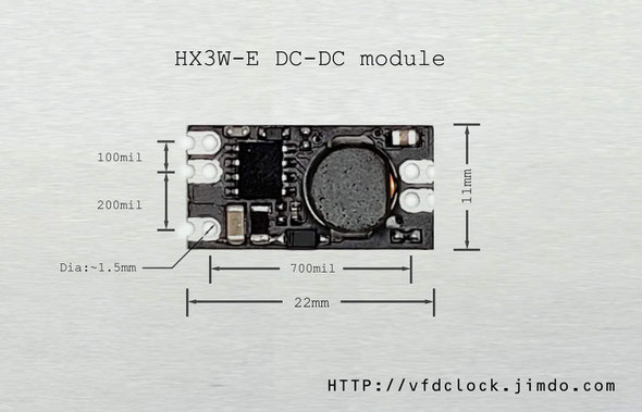
1.In SMD type,only one side of the PCB contains equipments,very thin.Half holes on left&right
side for soldering on PCB as a PSU module on board,also contains Full holes for adding male/Female pins as plug-in module.
2.Please note that the EN pin in this SMD module is not an optional pin,please connect it with a MCU GPIO or connect it to +3V3/+5V to turn the Module
power on(If can add a pull-up resistor (like 10k) to +3V3/+5V will be great);
3.With optional ADJ pin,can adjust the HV output with adding an extra resisotr,HV output adj. range in [~80V~~170V] range.if driving NIXIE tubes only,can connect ADJ pin to GND,the module will
output ~170V;
DANGER! Lethal Potentials
Present
THIS MODULE CONTAINS DANGEROUS, HIGH VOLTAGE
POTENTIALS. USE CAUTION.
DO NOT TOUCH ANY PART OF THE MODULE WHEN IT IS WORKING.
Tips:
1. Standard 0.1"(2.54mm) pins, easy to be used, can use bread board or DuPont-Wires etc.
2. Please control the input current <=400mA for the low heat working state;
3. Module contains over current protection+soft boot-up. When over heat, the module will turn off, you need to re-power on to reset the module;
4. We recommend working under 5V only,no over 6V.
5. More stable HV output, even for the heavy loader, the max output voltage only get a little bit drop;
6. If one module's power is not suited for your app,use two or more modules for driving the separated NIXIE tube(s) group,etc.;
7. Do not connect the modules' outputs in "Parallel Connection"!!!
Specifications(For reference only):
Module Size : 22mm(L)*11mm(W)*~6.4mm(H);
Module Pins : Half holes in 0.1"(2.54mm) std. gaps;
PCB Color : Black;
Freq: ~85kHz;
Pin Functions
|
ID |
Name |
Description |
|
0 |
Vcc/+5V |
Input supply voltage, 4.5V to 12V.(Recommend 5V only, no over 6V) |
|
1 |
GND |
Ground |
|
|
|
|
|
3 |
HV |
High voltage output. +170V(+-5%) |
|
4 |
EN |
Enable pin for turning the module ON/OFF |
|
6 |
ADJ |
add extra resistor to Ground can adjust the HV output from [~80V~~170V] Range,(Optional,if no use,connect to GND,module will output ~170V) |
*EN pin can be controlled by MCU GPIO[*3V3 or 5V MCUs are all fine]) directly,no need to add resistor in serial.
For 24*7 continually working condition, we recommend you control the input current less than 400mA when under 5V in, it keeps this module working under the low heat condition.
Typical Usage:
For driving NIXIE Tubes;
Tue
25
May
2021
5V Ready-HV5WAC-E New HV NIXIE module with DC+AC output
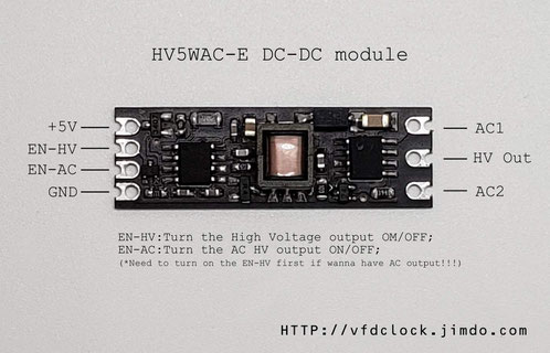
NEW-[HV5WAC-E]-Smaller HV5W with DC+AC output HIGH VOLTAGE
NIXIE POWER SUPPLY MODULE PSU-NIXIE TUBE ERA
Same Like Normal HV5W module but with an extra HV DC2AC convert circuit
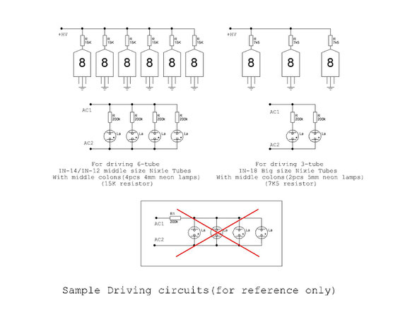
inside it.Now can output not only HVDC but HVAC for driving the neon lamps(To light two pins up inside the neon lamps).

We recomment using this module for driving 6tube IN-14(or in12 etc.) +4pcs neon lamps as middle colons or Driving 3tube IN-18 nixie tubes+2pcs neon lamps (thus for 6tube IN-18 nixie clock ,u need two of this module),the +HV DC output is for driving Nixie tubes and AC1+AC2 HV output is for driving Neon lamps as middle colon,thus two pins inside neon lamps all can be light up because of we are using AC HV to drive it.
1.In SMD type,only one side of the PCB contains equipments,very thin.Half holes for soldering on PCB
as a PSU module on board,also contains Full Round Holes for users to add Male/Female Pins as a plug-in module.
2.Please note that the EN-HV and EN-AC pin in this SMD module is not a optional pin,please connect it with a MCU GPIO to control it or directly connect to +3V3/+5V to
turn the Module power on;
DANGER! Lethal Potentials
Present
THIS MODULE CONTAINS DANGEROUS, HIGH VOLTAGE
POTENTIALS. USE CAUTION.
DO NOT TOUCH ANY PART OF THE MODULE WHEN IT IS WORKING.
Tips:
1. Standard 0.1"(2.54mm) pins and SMD half holes, easy to be used, can use bread board or DuPont-Wires etc.
2. Please control the input current <=800mA for the low heat working state;
3. Module contains over current protection+soft boot-up. When over heat, the module will turn off, you need to re-power on to reset the module;
4.We recommend working under 5V only,no over 6V.
5. More stable HV output, even for the heavy loader, the max output voltage only get a little bit drop;
6. If one module's power is not suited for your app,use two or more modules for driving the separated NIXIE tube(s) group,etc.;
7. Do not connect the modules' outputs in "Parallel Connection"!!!Do not Connect The +HV putput pins with AC1/AC2 pins, do not short HV And
AC1/AC2 pins!!!
Description:
HV5WAC-E is a newly designed high voltage module, it works under 5V USB power, with ~170V
DC output via +HV pin and HV AC output via AC1+AC2 pins,(especially designed for driving the NIXIE tubes. The max power
output is enough for lighting up 8PCS IN-14 NIXIE tubes(Or 4PCS IN-18 with
all segment "8" been light up) + 4PCS NE-2 neon bulbs. Low EMI and with No audible noise.
It contains an ENABLE pin to turn the module on/off, and
can be controlled by an regular logic signal, like a MCU's GPIO PIN(3V3 or 5V MCUs are all fine).
Pictures/Video(s) of the module
(For reference only):
Specifications(For reference only):
Module Size : 37mm(L)*11mm(W)*~6.4mm(H);
Module Pins : Half holes in 0.1"(2.54mm) std. gaps, output part in 0.15#;
PCB Color
: Black;
Freq: ~85kHz;
Pin Functions
|
ID |
Name |
Description |
|
0 |
Vcc/+5V |
Input supply voltage, 4.5V to 12V.(Recommend 5V only, no over 6V) |
|
1 |
EN-HV |
Enable pin for turning the +HV output ON/OFF |
|
2 |
EN-AC |
Enable pin for turing the AC1+AC2 output ON/OFF(The EN-HV pinmust be on first) |
|
3 |
GND |
Ground |
|
4,6 |
AC1+AC2 |
High voltage AC output ;~170V (+-10%) |
|
5 |
HV |
High voltage DC output. +170V(+-5%) |
*EN pin can be controlled by MCU GPIO[*3V3 or 5V MCUs are all fine]) directly,no need to add resistor in serial.
For 24*7 continually working condition, we recommend you control the input current less than 800mA when under 5V in, it keeps this module working under the low heat condition.
And this module is also suite for driving 6 tubes IN-18 clock, you just need to use two modules for driving it. Each module can drive 3PCS IN-18 tubes + 2PCS NE-2 neon bulbs (as dots) with no problem.
Typical Usage:
For driving NIXIE Tubes;
When under heavy loader,eg:output over
18mA,under 24*7 condition,the Max temperature of the transformer is about: Room temperature+20℃;Other parts get almost no heat.
Sun
07
Feb
2021
How to make a fast testing PCB by using a CO2 laser cut
In this article we are going to teach you how to create a fast tesing PCB if u have a CO2 laser cut.
For small size testing PCB,it costs us less than 30 mins to get a working PCB.
First prepare a regulaer PCB made by factory with a clean area that contains flat copper under the Green UV painting as u can see in the pic.
In this sample,we use an old Li-ion battery PCB which we designed for installing battery for our IN-18 SD clock PRO. It contains enough space to create our testing PCB.
We are using EAGLE PCB V6 software, now export the first mask picture.
As u can see in the TOP pic,first,display only [TOP]+[PADS]+[Vias]+[Dimention] layers only.

Then export the first mask pic to a BMP file,by using export -> image function as u can see in the picture.
We use 1200dpi high resolution and output [Monochrome] BMP file.
Here is the output a.bmp mask file. Then import the BMP file to ur Laser Cut Software to burn it to the PCB.
We are using a 40W 3040 Co2 laser cut machine,only need to set 7%~10% output laser power, this power is enough to burn the green UV painting layer from the PCB surface.
After washing the PCB surface,we can goto the etching PCB part.

In eaching part,u can use:
1. Use traditonal FeCl3(direty);
2. Use mixture of hydrogen peroxide (H2O2) and hydrochloric acid (HCl) in about water+H2O2+HCl=1:1:1 ratio; (Fast,but damgerous);
3. Use Sodium persulfate (Na2S2O8);(the key is the temperature and pumping air bulb in);
After the PCB is being etched,need to remove the green UV painting on its surface.if u do not need any of the green painting on it,u can use sandpaper to remove all of it. But we can do it in more elegant way as u can see later.

Let us output another mask that contains the [Pads]+[Dimention]+[tCream] layers.
The problem in this step is the cream parts are not displayed in solid color,we need to change the layer setting to make it displays in solid way.
Double click the bar near "31[ ]tCream" in the layers list,change it to solid color.As u can see in the picture,no need to care about the color because we will output the mask into mono in the next step.

Do the same step to export it to a BMP file in 1200dpi, monochrome as u have done before.

Here is the output b.bmp mask file. Then import the BMP file to ur Laser Cut Software to burn it to the PCB.
Then all the parts that need to be solder will be appeared without green painting.
TIPS:
If need to drill holes,we recommend u do it before etching.
If need to get more HQ result,do Co2 laser focus calibration first;
If u want to output the PADs in Solid with no middle hole,please change the setting shows in blow picture.
Coating a layer of black painting on regular cu PCB surface also works fine.Pics shown blow.


Thu
21
Jan
2021
5V ready OLED-1602 module for ARDUINO via IIC
You can find the password of PDF inside the item parcel.
OLED1602 Module for
Arduino /AVR/PIC/STM/ARM/PI 5V ready
Specifications(For reference only):
PCB Size: 82mm*22mm;
PCB color: Green/Black;
OLED Panel Size: 68.5mm*17.5mm;
Active Area: 2.26";
Panel Color: Blue;
Weight: ~12g;
Supply Voltage: 3V3~5V;
1). 5V Supply + 5V IO;
2). 3V3 Supply + 3V3 IO;
3). 5V Supply + 3V3 IO; (!!!No recommend! On your own risk!!! May work with some STM32 MCU Pins that survive under 5V IO,recommend add 1K resistors in serial with IIC pins);
Max Current: ~100mA;
Port: IIC (4k7 IIC pull-up resistors on PCB.);
Pins:
VDD +3V3~+5V;
SDA: IIC data pin;
SCK: IIC clk pin;
GND: Ground;
--------Optional pins(May not exist,depends on PCB version!!!)-----
HVEN: turn HV on/off(Optional);
/RESET: reset pin(Optional);
The module works with any 5V DC MCU,especially designed for ARDUINO!
Features:
1). 5V Ready,easy to be used.Can connect to your ARDUINO UNO board with only 2 signal wires;
2). High Brightness,no heat;
3). All SMT components,very thin PCB,easy to be drived;
4). Contains over-current protection and reverse connection protection circuits;
5). Open source ARDUINO UNO source code,pure C code,easy to be used and ported;
For video(s):
HTTPS://youtu.be/i9q9lQ41UB0
For more information:
HTTP://vfdclock.jimdo.com
The source code is for ARDUINO UNO,running in ARDUINO V1.04.
Please use Acrobat Reader from ADOBE to open this PDF file,then you can find the source code in the PDF attachment.


Sun
22
Nov
2020
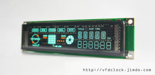
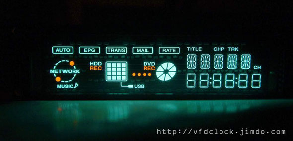
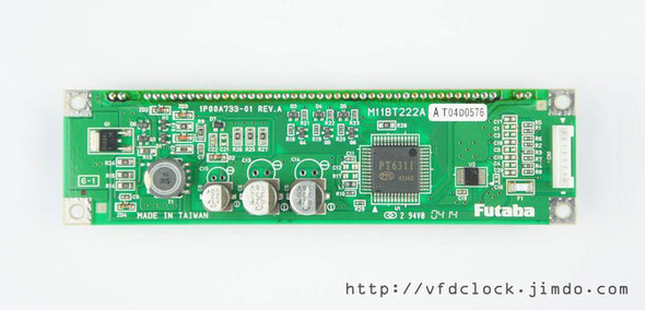
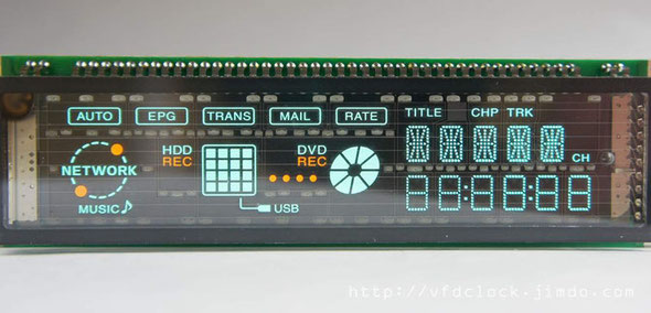
FUTABA M11BT222A VFD(Vacuum Fluorescent Display) Module
Outside link:
Have found C51 source code in:
https://blog.csdn.net/farmanlinuxer/article/details/78993335
Specification:
Module Size:150mm(L)*40mm(W)*20mm(T);
Socket Pitch:2.0mm*8pins;
App: Set-Top Box(STB)/HTPC/Video Player&Recorder;
Color:Green+Red;
Operating Condition:
Power
supply:5V DC;
Current: ~500mA;(5V,light up all the segments together.)
Pins definition:
1. VCC (+5V)
2. GND
3. NC(no connection)
4. EN(High:HV+Filament On; Low:Shut-down)
5. DIN
6. GND
7. /SCL (invert)
8. /STB (Invert)
Driver Chip:PT6311

Thu
14
Nov
2019
5V Ready-VFD Matrix Module for Arduino/STM32 etc.

Caution:
1.High Voltage(~100V) on board,do not touche any part of PCB with power on;
2.May have tiny sound when displaying that is from filament which is caused by internal driving IC inside PANEL in scanning freq; You can install the module inside an enclosure to reduce the sound;
Would please use Adobe Acrobat Reader to open this PDF file,and you can find source code zip file in the attachment part of PDF file.
For video: https://youtu.be/YXwZPGMiKqk
Panel Size: 150mm*48mm;
Panel Color: Green;
Supply: 5V DC;
Max Current: ~800~1000mA;
Module Size:~ 166mm(L)*62mm(W)*--mm(H);
PCB Size: ~166mm*62mm;
PCB Color: Black/Green;
Weight: ~--g;
Features:
1).5V Ready, easy to be used. Can connect to your ARDUINO UNO board with only 3 signal wires;
2).High efficiency power circuit, High Brightness;
3).All SMT components, very thin PCB, easy to be driven;
4).Logic part support 5V or 3v3 signal;
5).Contains over-current protection, and reverse connection protection circuits;
6).Open source ARDUINO NUO source code, pure C code, easy to be used, also provide a simple flip clock source code for ARDUINO UNO.
7).Simple 3-wire SPI interface, with EN pin, support shutdown the High Voltage and Filament Supply completely.
Interface:
3-wire SPI: DIN/CLK/LATCH(CS)
---------------------------
+5V (main power.)
GND
DIN
CLK
LATCH(mark:CS on PCB)
-------Other pins----------
+3V3 out 100mA (max) (optional)
INT-SYNC out (optional)
EN High voltage & filament supply enable(optional)
Logic part is 5V and 3v3 compatible.
Arduino fake flip clock source code in pure c;
For video:
https://youtu.be/YXwZPGMiKqk
Thu
14
Nov
2019
5V Ready-HLD026 VFD module for Arduino
Arduino Source code for ARDUINO UNO.
Compiled under ARDUINO V1.0.4 in pure C code.
Please use ACROBAT reader from Adobe to open the PDF file and find Source code files in attachments part of PDF.
You can find the password of PDF inside the parcel.
Specifications(For reference only)
VIN:5VDC/~150mA
Panel size: 106mm*25mm
PCB size: 116mm*32mm
Color: Green
Display:SEG * 10
Driver Chip: PT6312
Features:
1).5V Ready, easy to be used. Can connect to your ARDUINO UNO board with only 3 signal wires;;
2).High efficiency power circuit, no transformer, no heat, Low HV, very safe, High Brightness;
3).All SMT components, very thin PCB, easy to be drivered;
4).Contains over-current protection, and reverse
connection protection circuits;
5).Open source code for ARDUINO NUO, pure C code.
6).Simple 3-wire SPI interface, with EN pin, support shutdown the High Voltage and Filament Supply completely.
Interface:
3-wire SPI:
DIN
CLK
LATCH(CS)
+5V
GND
EN - HV supply enable(optional)
For Video:
https://youtu.be/0dTg2ngvf1c
For video(s):


Thu
31
Oct
2019
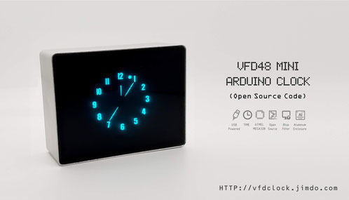
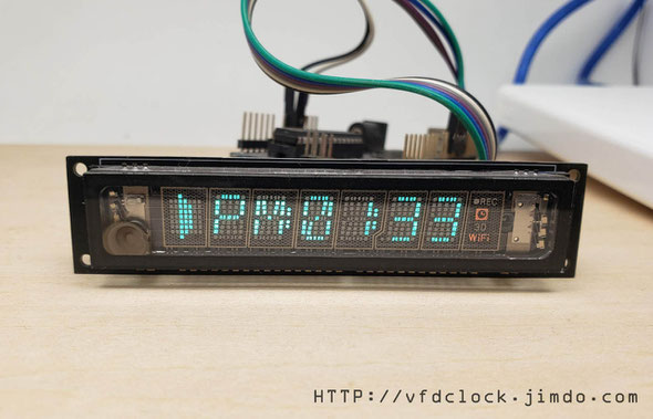
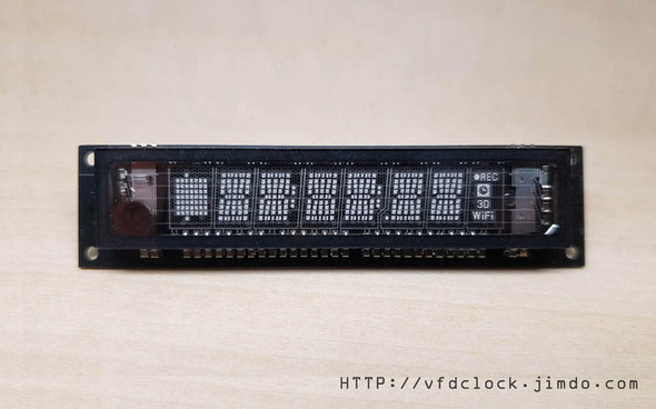
Arduino Open Source-USB-VFD48 MINI DIY Clock Assembly Instructions

VFD48 MINI
Pure C source code for Arduino V1.0.4
Please use ACROBAT READER to open it or you may not be able to get the attach file inside it.
Please select ARDUINO UNO board in arduino compiler.
if can not open pdf attached file,would please send us a email,we will send u src directly,u can gind our email address inside pdf file.
First,solder the front side of PCB, It contains few equipments on this side,please double check the direction of the PT6315 Chip before soldering it on PCB.
Recommend glue the chip on PCB by using tape before soldering.
Remember tin the middle pad of the CR1220 battery socket,and check the direction of the battery socket.
Plug the CDS sensor near the PCB or it will effect the VFD48 panel installtion.

Most of the equipment on the back side of the PCB,please solder it carefully.
1)Solder the MCU part first and the crystal part,please double check the direction of MCU and solder the crystal fast,other small resistors and caps are easy.
2)solder the -HV part on the right bottom side and filament driver part on the top bottom side,same as the prv. step,please double check the IC direction and solder fast.


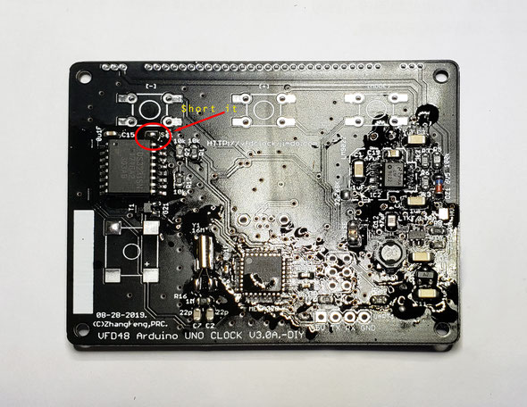
3)Solder the RTC part on the top-right side of the PCB,in this part,remember to short the small pad on the top of the RTC chip, this pad is for the 5V supply of the RTC chip, if you left it open, the RTC chip will not work.
4) Solder the USB socket on PCB,please also remember to solder the left and right holes part of the usb soket as shown on the pic.
Give it a double check of all the components, if all fine ,we can do a test to see if the PCB in working.
We plug the VFD48 panel on the PCB,press it to make all its legs touchs the holes, then plug the USB power on,if all fine,the VFD48 panel will in running. It will be light up,and the time will ticking.
!!!Do not solder the VFD48 panel on if the circuit did not work!!!
If all fine,you can wash the PCB to make it clean.

Then we will solder the rest components on the PCB.The keys and buzzer can not be washed,thus we nned to solder these things in the last step.
5) cut the keys' legs short then plug it on the PCB,you can solder it on the top or on the bottom side of the PCB.

6)Solder the buzzer on the PCB,please double check it's direction,check the [+] pad.

7) Plug the VFD48 panel on the PCB,power on ,recheck all things again,if all fine,you can solder the VFD48 panel on.
Tips:you can older the left one leg first then adjust the installtuon height of the panel,then solder the one leg of the left side. if all fine,then you can sut all the legs short,solder all the rest legs on the PCB.
After assemble the PCB,we recommend you do at least 48Hours heat testing,if all fine,then we can install it in the aluminum enclosure.

Aluminum Enclosure Assembly Instructions

First install the 5mm Copper column as shown in the pic.
Then glue the blue filter on the VFD48 panel by using double-side tape.Recommend glue on the top and bottom side.
The blue filter contains protective film on both side,remove it before you use it.
Now install the PCB into the aluminum enclosure. Then glue the front panel on by using the double-side tape on its surface.
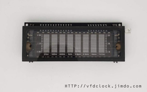
Done!
Tue
29
Oct
2019
GTF07 Dot char VFD display module with ARDUINO C source code

Arduino Source code for ARDUINO UNO.
Compiled under ARDUINO V1.0.4 in pure C code.
Please use ACROBAT reader from Adobe to open the PDF file and find Source code files in attachments part of PDF.
Specifications(For reference only)
VIN:5VDC/~150mA
Panel size: 85mm*16mm
PCB size: 100mm*20mm
Color: Green
Display:[5*7 dot] 7chars.
Driver Chip: COG
Features:
1).5V Ready, easy to be used. Can connect to your ARDUINO UNO board with only 3 signal wires;(Logic part supports 5V or
3V3 logic with no problem);
2).High efficiency power circuit, no transformer, no heat, Low HV, very safe, High Brightness;
3).All SMT components, very thin PCB, easy to be drivered;
4).Contains over-current protection, and reverse connection
protection circuits;
5).Open source code for ARDUINO NUO, pure C code.
6).Simple 3-wire SPI interface, with EN pin, support shutdown the High Voltage and Filament Supply completely.
Interface:
3-wire SPI:
DIN
CLK
LATCH(CS)
+5V
GND
EN - HV supply enable(optional)
For video(s):


Tue
10
Sep
2019
VFD48 Aluminum enclosure assembly instructions

You can find this enclosure from our ebay store.
Please check the links on the right-top of this webpage to visit.
Specifications(For reference only):
Enclosure Size:90mm(L)*66mm(W)*24mm(H)
Before you start to assemble the enclosure,please double check the 1mm gap pic of PCb on the pic to see if your VFD48 clock FITs,99% of our vfd48 clock PCB are all fit with no problem,the buzzer beep-hole may face to top-side or left-side,all work.
First install the 5mm Copper column with 2pcs plastic gaskets as shown on the pic, Do not scrow too tight,may need adjust the distance a little bit when plug in the enclosure.
!!! Total high of the bottom side of the PCB is :
5mm(Copper column)+1mm(gasket)+1mm(gasket)=7mm;
Because of we do not know how high you have installed the VFD48 clock panel,you can install only 1pcs or none of the gaskets to make sure that when the vfd48 clock PCB be installed inside the enclosure, you can still install the acrylic panel on with no problem,and all 3pcs of buttons can be pressed on the back side.
Plug the VFD48 clock PCB in the enclosure,make sure all 4pcs of Copper column be plugged inside the 4 holes. If all fine,you can add a little bit of epoxy in the 4 holes to glue the Copper column inside the enclosure, and then wait untill the epoxy becomes solid.
Then glue a short of paragraph transparent double-side tape on the top edge of the clock panel,as you can see in the picture,we will need to glue the blue filter in next step.

The blue filter contains protective film on both side,remove it before you use it.Then glue the blue filter on the VFD48 panel.
Tips:In some of version,you can also try to glue the blue filter on the middle of the front panel.

Now you can install the front panel. On the back side of the front pancel contains Double-side tap to glue the pancel on the enclosure,and after be installed,you can remove the protective film on the front side.

Tue
20
Aug
2019
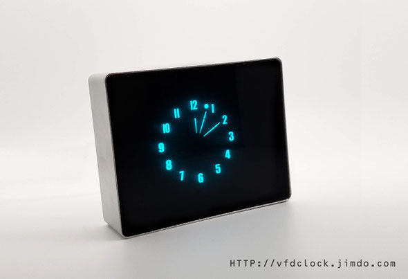
USB Powered IN-18 Single Digit NIXIE Clock Pro

For PDF instructions,check:
USB Powered IN-18 Single Digit NIXIE Clock with Aluminum Enclosure V1.0.
IN-18 Single Digit NIXIE Clock with aluminum enclosure
Brand new,I designed and made it by myself.
Notice:
In order to drive the NIXIE tube, some
internal equipments are under the High Voltage(up to 180V DC),please do not use this clock outside or in any wet conditions,please do not touch any part inside the clock when power supply is
turned on.Always keep it away from kids.
Specifications(For reference only):
Tube Name: IN-18 (Made in the U.S.S.R.);
Tube Size:30mm(dia);
Tube Height:68mm(no including the legs and the glass
nipple);
Digit Height:40mm;
Digit Width:22mm;
Clock Supply: 5V DC via MINI-USB;
Working Current: ~250mA(Without Li-battery)/~450mA(With Li battery in charging);
Clock Size:60mm(L)*60mm(W)*25mm(H*without NIXIE tube)
PCB Size:54mm*54mm;
PCB Color: Green or Black;
Weight:~128g(weight with the tube installed);
The clock works with any standard USB power supply,use only high-quality adapter!
Features(For reference only):
You can replace the tube by yourself without using any tools.
1). 5V USB powered,easy to be used. Can
connect to your computer's USB plugs directly.
2). Support 12H or 24H display modes, can show "."as“A/P" in 12H time format.Leading zero blanking is programmable.
3). Display date in all format: YY.MM.DD or DD.MM.YY or MM.DD.YY or even MM.YY.DD.
4). Support different Effs:Normal/Fading/Cross Fading/Slow Fading/Loop for displaying time.
5). High accuracy DTCXO (temperature compensated crystal oscillator) inside,+-4.94 seconds(MAX) per month.
6). Simple setting by using 2 buttons only and supports IR remote control(optional).
7). Three alarms with weekends ON/OFF support,can be controlled individually.
8). Three programmable Auto Power ON/OFF mode,can turn ON/OFF NIXIE tubes in any time you want.This function can save tubes life.
9). 8-level adjustable NIXIE tube bright with Auto-brightness feature(its ability to adjust the tube brightness depending on the current environment).
10). Rechargeable Backup Battery or Farad capacitor Or CR1220 battery keeps RTC running during power outages.
11). Tri-colored RGB LED mounted under the NIXIE tube. This LED can display any color with a lot of predefined auto color change effects.
12). Store user settings in non-volatile memory.
13). Beautiful CAD designed ,CNC made aluminum enclosure makes the clock look beautiful. You can assemble/disassemble the case by using only 4 screws on the bottom of the case.The case
also has 4 bumpers as feet on the bottom of the case in order to stop to prevent case's damage.
14). Support temperature sensor(optional).
15). Support wireless GPS time sync receiver(optional).
16). Supoort Li battery function(optional).
For video(s):
For more information visit:
vfdclock.jimdo.com

For Instructions:
Please visit the url in
the bottom side of the pictures to get the PDF instructions,
etc.

more info...


Mon
01
Jul
2019
USB powered-B7971 6-tube NIXIE clock
Instructions:
Tue
11
Jun
2019
USB Powered 6E1P(EM80) 2-tube Magic Eye VU Meter(Stereo Audio Visualizer)-V1.0
6E1p 2-tube vu meter


Tue
11
Jun
2019
USB powered-Z566M Single Digit NIXIE Clock
Z566m Single digit NIXIE clock
-------------------------------------------------------------------------------------------------------
USB Powered Z566M
Single Digit NIXIE Clock with acrylic enclosure. -NO
TUBE
!!!This Item Contains No Z566M
TUBE.All you need to do is buy 1PCS Z566M NIXIE Tube and plug it in the socket by hand.
For review article(For
reference only):
Z566M Single Digit NIXIE Clock with acrylic enclosure
-----------------------------------------------------------------------------------------------------
Product Change Notification in the New Version:
Specifications:
Tube
Name:Z566M; <<<===Prepare the tube by yourself.
Clock Supply: 5V DC via USB;
Working Current: ~350mA;
Clock Size:58mm(L)*54mm(W)*80mm(H)
PCB Size:48mm*44mm;
PCB Color: Black;
Weight:58g(weight with the tube installed);
The clock works with any standard USB power supply,use only high-quality adapter!
Features:
You can replace the tube by yourself without using any tools.
1). 5V USB powered,easy to be used. Can connect to your computer's USB plugs directly.
2). Support 12H or 24H display modes, can show "."as“A/P" in 12H time format.Leading zero blanking is programmable.
3). Display date in all format: YY.MM.DD or DD.MM.YY or MM.DD.YY or even MM.YY.DD.
4). Support different Effs:Normal/Fading/Cross Fading/Slow Fading/Loop for displaying time.
5). High accuracy RTC inside,+-13 seconds(MAX) per month.
6). Simple setting by using 2 buttons only and supports IR remote control(optional).
7). Three alarms with weekends ON/OFF support,can be controlled individually.
8). Three programmable Auto Power ON/OFF mode,can turn ON/OFF NIXIE tubes in any time you want.This function can save tubes life.
9). 8-level adjustable NIXIE tube bright with Auto-brightness feature(its ability to adjust the tube
brightness depending on the current environment).
10). Rechargeable Backup Battery or Farad
capacitor keeps RTC running during power outages.
11). Tri-colored RGB LED mounted under the NIXIE tube. This LED can display any color with a lot of predefined auto color change effects.
12). Store user settings in non-volatile memory.
13). Beautiful CAD designed acrylic case made using a laser cutter makes the clock look beautiful. You can assemble/disassemble the case by using only
4 screws on the bottom of the case.The case also has 4 bumpers as feet on the bottom of the case in order to stop to prevent case's damage.
14). Support temperature sensor(optional).
For Video(s):
https://youtu.be/UuLHPXgxT3I
For Instructions:
Please visit the url in
the bottom side of the pictures to get the PDF instructions,
etc.
For more information and newest instructions,please visit:
Contains:
1. 1PCS fully
assembled clock(with NO Z566M NIXIE tube,all installed in an acrylic case,with USB
cable), ready to go,just plug your IN-18 tube in it,and connect with the USB power.
Power adapter is not included, any USB adapter may suit,or you can connect it to the USB ports in your
computer.
Optional extra:
1.For the IR Remote Control Function(With 1PCS Remote Control ): +5.99 USD;
2.For the Temperature Sensor Function:+5.99USD;
3.For an extra acrylic case with all screws,bumpers,etc. as backup:+5.99USD;
4.For 1PCS Brand 5V/1A USB Power Adapter: +5.99 USD;
Battery is not included!!!(We can't ship the battery in the mail package,so the IR remote control battery(1pcs CR2025) may not be included,you need
to prepare it by yourself.)
Notice:
Please note that we need about 3~5 working days for assembling it after payment is received.
We may will change the Outlook/Circuit/PCB/Components without notification!
Payment methods:
We ONLY accept PayPal on eBay
selling, other payment is not acceptable.
Please PAY within 7 days, or we'll re-selling the item.
Shipping:
We ship to American via ePacket Delivery with tracking number;
We ship to Other countries/locations via International Economy Package with tracking number;
For shipping to The United Kingdom or Australia or Russian Federation, we strongly recommend you update to the
EUB(express);
Price for updating to the EUB(express):
For shipping to The United Kingdom or Australia: +5.99usd;
For shipping to Russian Federation: +3.99usd;
Shipping time:
10-20 working days for ePacket Delivery to the U.S.A.(normally you will receive it in about two weeks), depends on the
destination location;For other far locations may need more days.
Please note that International Economy Package can ship to the World wild with low price,but
the transport speed is very unstable,mail delay is very normal,shipping to far locations may
cost over 30 days,sometimes the cargoes will be stacked in the airport for over one month(especially in the special meeting time,it
happened before).
Please understand that we can't control the mail speed.If the mail delayed,please be patient.
If you wanna save your time,add extra money for updating to the EMS.
We ship to your PAYPAL Verified Address only;
Any import tax or charges should be paid by the buyer.
Tips:
About the Economy
Mail to the World Wide:
The International Economy Package is mailed to the destination country by CHINA POST and delivered via the local
postal system. Delivery time is usually between 14 to 30 business days.
Usually delivery status is traceable on the post office website of CHINA POST and(or) the destination country post office website.
Mail tracking
website:
But sometimes,on those web sites,you can track 0 info or just the info that when the goods are transported inside CHINA. Especially shipping to the far locations,just be patient.
For the Economy Mail,if we got the Tracking number for you,it means that the goods are
already in the post office.
If you have not received the goods in 30 days,notice us,we will ask for the detail tracking information
via the local post office.


Sun
02
Jun
2019
SLIM-8W-High Voltage Power Module-12Vto170V-MC34063-OpenHardware

Eagle source Files are inside the PDF file blow,please use Acrobat reader from adobe to open the PDF file,will find all files inside attach part of PDF. Others PDF reader may not be able to find the attached files inside PDF.
When save the attach file,Please rename the SLIM12D.rar.txt back to SLIM12D.rar, then open it with winrar.
You can find the password of PDF inside the parcel.
The Module can light up 6~8pcs IN-18 NIXIE tubes at the same time.
New-Slim 8W-34063 Based High Voltage for NIXIE
1.High efficiency,High power,up to 8W(Max);
2.Small size PCB,29.5mm(L)*16mm(W)*7mm(H) only;
3.Highly optimized circuit, high quality key components;
4.Open hardware design;
THIS MODULE CONTAINS DANGEROUS,
HIGH VOLTAGE POTENTIALS. USE CAUTION.
DO NOT TOUCH ANY PART OF THE MODULE WHEN IT IS WORKING.
Tips:
1. Please control the input current in <=0.8A for the low heat working state,if need more power output,you can increase the input voltage;
2. Please use high quality and stable input DC source,make sure no over the MAX input voltage;
3. Module contains input reverse polarity protection;
4. For the heavy loader,the max output voltage may get drop,it's normal;
5. Module contains an optional /EN pins to turn the module HV output ON/OFF,can be controlled by 3V3 or 5V mcu GPIO; when set this pin to H,will turn the module HV output off,when float or set to L,the module
will back to work;
Description:
This high voltage power converters are typical boost converters
based on 34063 chip which can accept 10 to 15V DC input,and output up to ~170V DC
.
We recommend work with 12Vin,and with <8W output;
Typical
Usage:
For driving NIXIE Tubes.
Typical Parameters:
(For reference only)
Input: 10V~15V DC, recommend 12V;
Output: ~170V DC;
Output
Current(MAX): 40mA;
Max Power
Intput: 8W;
Module size: 29.5mm(L)*16mm(W)*7mm(H); (~7mm height contains bottom equipment+PCB+top equipment
total).

Mon
20
May
2019
DIP-USB Powered-4-Tube-Arduino NIXIE Thermometer-Open Hardware
For assembling instructions,please check:
https://vfdclock.jimdo.com/2017/08/01/thermometer/
We add an extra IV-19 NIXIE tube to display [+]&[_]&[~],based on the 3-Tube NIXIE Thermometer design,others are all the same except the source code.
You can find the password of PDF inside the KIT BOX.
Please use Acrobat Reader from ADOBE to open the PDF in the page,or you may not be able to get the attached files inside the PDF if using other PDF reader!!!

Add-ons:


1mm grid of topside of PCB
Sun
19
May
2019
5V Ready-HL76W 5*7 dot char VFD display module for ARDUINO-5V Ready

Arduino Source code for ARDUINO UNO.
Compiled under ARDUINO V1.0.4 in pure C code.
Please use ACROBAT reader from Adobe to open the PDF file and find Source code files in attachments part of PDF.
Please use Acrobat Reader from ADOBE to open the PDF in the page,or you may not be able to get the attached files inside the PDF if using other PDF reader!!!
Specifications(For reference only)
VIN:5VDC/~250mA
Panel size: 110mm*21mm
PCB size: 120mm*30mm
Color: Green
Display:[5*7 dot] 13chars.
Driver Chip: PT6302
Features:
1).5V Ready, easy to be used. Can connect to your ARDUINO UNO board with only 3 singal wires;
2).High efficiency power circuit, no transformer, no heat, Low HV, very safe, High Brightness;
3).All SMT components, very thin PCB, easy to be drivered;
4).Contains over-current protection, and reverse connection
protection circuits;
5).Open source code for ARDUINO NUO, pure C code.
6).Simple 3-wire SPI interface, with EN pin, support shutdown the High Voltage and Filament Supply completely.
Interface:
3-wire SPI:
DIN
CLK
LATCH(CS)
+5V
GND
EN - High voltage & filament supply enable(optional)
(Tips:Some of the version may contain a test vias on PCB,just need to short the test 2pins then 5V poer on(please unconnect others pins) ,the module will do self testing.)
For video(s):

Sat
04
May
2019
DIY KIT-5V USB Power-Pluggable IN-18 6-tube NIXIE clock-Assembly Instructions
5V USB Powered-IN-18 6-tube Clock DIY version
Assembly Instructions
V1.0
Notice
For assembling this NIXIE KIT you need to have the skill of soldering DIP& SMD components. We use a Hakko FX-888 Soldering Station (with CF2 Iron Head). We use 183℃(degree C)low melt
temperature solder wire S60, 0.5mm(Dia.), Brand Almit.And for most of the SMD components are big size and easy to be assembled,if you have a Hot air blower station,will help.
For how to solder the DIP components, we recommend:
https://www.hakko.com/english/tip_selection/type_bc_c.html
https://www.hakkousa.com/video/
For how to solder the SMD components, we recommend:
https://www.hakko.com/english/tip_selection/type_bc_c.html
https://www.hakkousa.com/video/
Please do not change any equipments of the KIT or you may not be able to get the KIT in working.
Because it most of SMD components are big size, so it is very easy for you to assemble, we recommend to check the circuit diagram carefully and follow the steps shown blow.
We do not recommend you to solder the components in random order or if it has problems you will need more time for de-soldering(*Will damage the PCB Pad) and debug, we recommend you follow the steps in this instructions that you can do part test after finished each step.
For more info & update, please visit HTTP://vfdclock.jimdo.com
Or contact us: zjjszhangf@gmail.com
Thanks for choosing our product.
Building it
Well, because of the circuit is block based and not very complicated, all you need to do is get all the components in the right position and make sure no short or no float before you plug
the power in. We will show the soldering steps blow.
Preparing
1. Please print out the PCB installation diagram by yourself, the Circuit diagram is no need for soldering job, print it or not depends on you(Note: May only have the paper circuit
diagram in the KIT with no digital version provide.);
2. Check all the components in the kit bag, make sure nothing is missing (You can do this on a A4 white copy paper);
3. We recommend using a soldering station and small soldering tip for soldering this kit (we use F2 or CF2 type tip). We recommend using ~180℃ type soldering tin for this job. Please do
not use the high temperature soldering tin in this project or you will damage components or the PCB;
Please always remember that in this new version,only LEDs and NIXIE PINS and comma PINs are installing on the TOP side of PCB,others are all on the bottom side of PCB.
And double check the component before you solder it on PCB, and also double check its' direction for some diode and caps etc.,DO not go wrong,because of if go wrong,de-soldering DIP components are not very easy, may damage the PCB pad.
1): Middle comma Pins and HV module Pins
We need to solder some pins in this step,please solder it in this step,will be easier to be installed.
The first PINS are middle comma female pins,please plug the Female PINs on the top of the PCB then cover a had board like a small PCB or
small wood board etc.over the PINs, use two clamps to hold it with the main PCB, then flip the PCB. Now you can solder on the other side.
Tips: Because of the PINs are through hole version, please solder it carefully and do not let the tin goes in to the inside of the pins or will damage the PINs. If necessary, you can plug a
wood/bamboo toothpick in the bottom of PINs hole when soldering.
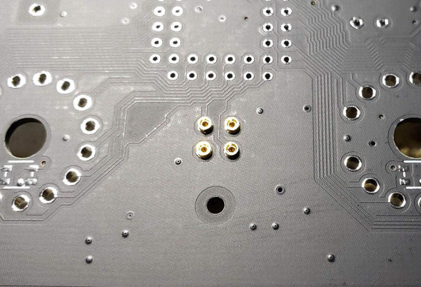
Test

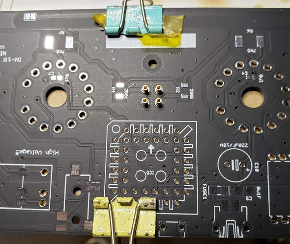
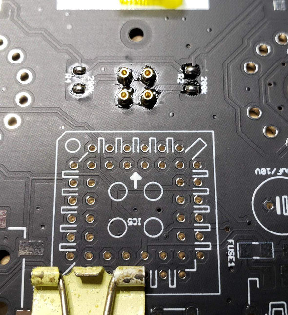
We have two types of HV moudles,for the SMD version ,you just need to solder it on the SMD PAD on the bottom side of PCB.
For the DIP version of HV moudle, we recommend you install it by using the female pins.
Please remember to install these pins on the bottom side of PCB,and use the same soldering methord same as the middle colon pins.

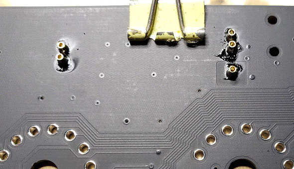
2): Middle comma Pins and MCU IC socket pins
Then solder the MCU IC sockt on the bottom of the PCB,this part is easy,just plug the IC socket in the PCB,flip it and press it on the table,then solder it. Please take care of the direction of the IC socket(check the first leg mark of the socket), do not go invert and do not go wrong PCB side.
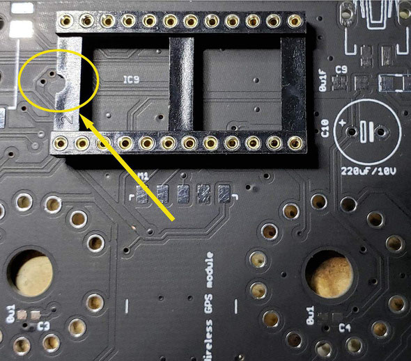
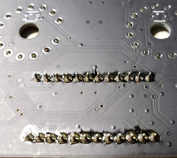
The PLCC44 SOCKETs, please take care of the first leg!!!
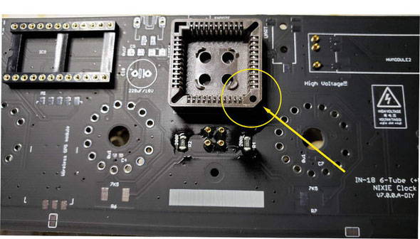
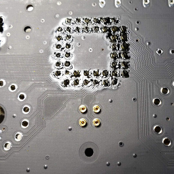
Tips: In order to protect the components like sockets, you can use aluminum foil to cover it's surface when you are using Hot air blower station to install the components near by.
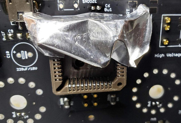
3): Install LEDs
The LED part contains 6pcs LEDs(With Chip inside it) and 6pcs 0uF(100nF) caps; Please note that the LED should be installed on the top side of the PCB, and take care of the first leg of the LED(The first leg is on the right-bottom side of LED with a tri. mark, and the LED pad has a white [.] to point out the first leg on PCB); Please solder the LED fast to prevent its be damaged;
Please solder the LEDs in low heat and solder it fast!!!
Do not forget to solder the 0u1(100nF) capacitor(s) near LEDs in this part on the bottom of PCB;

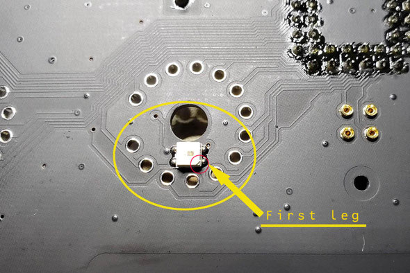
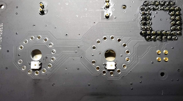
4): Install Main power and others components
The main power part has a USB socket(May in MINI USB/Micro USB),and a fuse, a 100nf cap and a Big Aluminum Electrolytic Capacitor(Please take care of it's direction).

Rest components are easy,please check the pic shown blow.
Notice:
For the CR1220 battery socket, please remember to tin the middle pad first and take care of the direction of the socket.
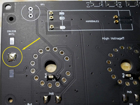

5): IN-18 PINS
Now we are going to solder the IN-18 PINS.Please flip the PCB to the front side,the PINS need to be installed on this side and please solder it on the middle part of the PINs;
First we recommend you plug the PINS in the IN-18 legs,then plug ALL the PINS to the install holds,plug it down to the middle part, then flip the PCB ,solder the PINs on the bottom side of PCB;
!!!Plase double check to see if all PINs are plugged to the middle part before you solder the PINs!!!

Plug down to the middle part of the PINS
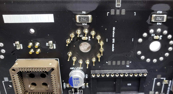
Flip the PCB,then solder the PINS on the bottom side of PCB

In soldering the PINS,if necessary,you need to keep pushing the tubes down to make sure all the PINS have been soldered on the middle part, please trade care of this part.
!!!Pleas note, do not add too much tin in soldering PINs,and please solder it fast. If add to much tin, the tin may go inside of the PINs and will solder the IN-18 tube legs with the socket,which will be big problem. We recommend add a little bit body lotion or oil on the surface of all in-18 PINs, will help to prevent be soldered together with socket.

And after finished soldering on tube PINS,give it a power on test(*Remember to plug the MCU module and HV driver Chips and HV mpdules in socket for testing) to see if have any problem.
6): Power ON Test
After finished all the steps shown up, please recheck it to see if has errors on the PCB.
Then plug the two PLCC HV driver Chips and Main MCU module and HV modules in the sockets; please double check the direction of IC and module
before power on, do not go wrong direction.
Now we can plug the 5V(At least 1A5) power in, if all fine, the NIXIE tubes will display the time.We recommend plug one NIXIE tube in when in the first time power on test, if first NIXIE tube
works, you can go power off and add another one, do test again...etc., until all 6 tubes are all in working;
If find errors or the the clock did not work, please go power off and re-check the circuit block by block to see if it has any short or float on PCB;
Step (8): Cleaning the Circuit Board
You can use the household rubbing alcohol and a toothbrush to remove the solder flux on the PCB.
If available, the anhydrous alcohol (used for electronics cleaning) works much faster. Blot the cleaned area with a non-linting tissue (like Kimwipes EX-L) or a clean towel or you can do it in your own way.
!!!Remember to remove the HV driver Chips and the MCU main board and hv modules(if in hv dip version) when cleaning the PCB!!!
You need to have a PLCC EXTRACTOR for unpluging the PLCC chip from the socket;
9): Buttons and Buzzer etc.
Because of Buttons and Buzzer etc. can not be washed, we need to solder 4pcs Keys and 1pcs Buzzer after cleaning the PCB.
If the Buttons are one side two pins version,just solder it directly on PCB,if the Buttons are two side 4pins version,cut one side 2 pins off buy yoursele,and band it flat the other side of 2pins then solder it and cut it short(or cut it short first before soldering);

It also has two 3.5mm plug socket,one is for GPS, the other is for "PIR Motion Sensor";Please remember to solder these on PCB too;
10): Create middle comma
For how to assembling the Middle comma,please visit:
KIT-Create the Middle Dot Comma for IN-18 NIXIE clock
You can make your own decision of the location of the bulbs in the middle glass tube.

Extras (10): misc extras
In editing...
Sun
21
Apr
2019
USB-Plug-able IN-8 6-tube NIXIE clock with glass tube middle dots
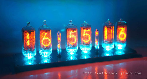
IN-8-2 Soft Leg 6-tube NIXIE clock,USBpowered.Pluggable


Sun
07
Apr
2019
Plug-able USB Powered,Two-Digit B7971 NIXIE Tube Clock

B7971 2-tube clock
Specifications:
Tube Name: B7971 ;<<<===Prepare the tube by yourself.
Tube Size:50mm(dia);
Tube Height:11.5mm(12.3mm with leg);
Digit Height:52mm;
Clock Supply: 5V DC via USB;
Working Current: ~660mA;
Clock Size:156mm(L)*80mm(W)*18mm(H)-(*no including the tube);
PCB Size:146mm*70mm;
PCB Color: Black;
Weight:~280g(weight with the tube installed);
The clock works with any standard USB power supply,use only high-quality adapter!
Features:
You can replace the tube by yourself without using any tools.
1). 5V USB powered,easy to be used. Can connect to your computer's USB plugs directly.
2). Support 12H or 24H display modes, can show "."as“A/P" in 12H time format.Leading zero blanking is programmable.
3). Display date in all format: YY.MM.DD or DD.MM.YY or MM.DD.YY or even MM.YY.DD.
4). Support different Effs:Normal/Fading/Cross Fading/Flashing/Loop for displaying time;Support 4 pre-defined Digit Fonts.
5). High accuracy DTCXO (temperature compensated crystal oscillator) inside,+-4.94 seconds(MAX) per month.
6). Simple setting by using 2 buttons only and supports IR remote control(optional).
7). Three alarms with weekends ON/OFF support,can be controlled individually.
8). Three programmable Auto Power ON/OFF mode,can turn ON/OFF NIXIE tubes in any time you want.This function can save tubes life.
9). 8-level adjustable NIXIE tube bright with Auto-brightness feature(its ability to adjust the tube brightness depending on the current environment).
10). Rechargeable Backup Battery or Farad capacitor keeps RTC running during power outages.(May install a CR1220 battery socket instead if can't ship battery,please prepare 1pcs CR1220 battery by
yourself.)
(!!!RTC battery/cap keeps the real time clock running for a while after USB power off,not keeping the whole clock running!!!)
11). Tri-colored RGB LED mounted under the NIXIE tube. These LEDs can display any color with a lot of predefined auto color change effects.
12). Store user settings in non-volatile memory.
13). Beautiful CAD designed acrylic case made using a laser cutter makes the clock look beautiful. You can assemble/disassemble the case by using only 4 screws on the bottom of the case.The case
also has 4 bumpers as feet on the bottom of the case in order to stop to prevent case's damage.
14). Support temperature sensor(optional).
15). Support Wireless GPS Module (optional), can sync time via wireless signal(*Need to have a GPS wireless time station as time signal sender);
16).Support PIR (human sensor module)(optional) to turn the clock ON/OFF by detecting the human body;

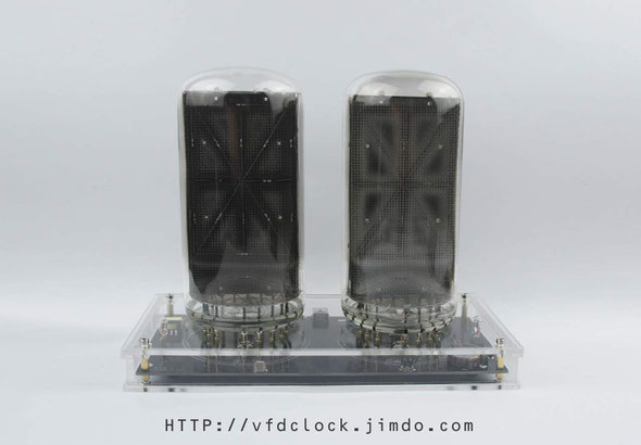
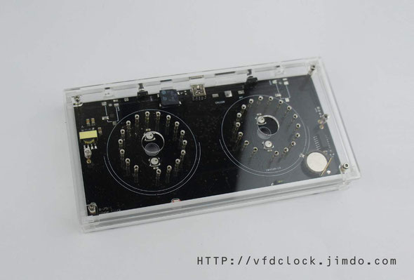
Sun
17
Mar
2019
Plug-able USB Powered,Two-Digit Z568M NIXIE Tube Clock
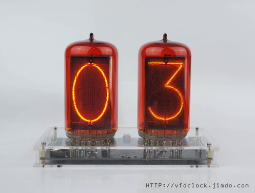
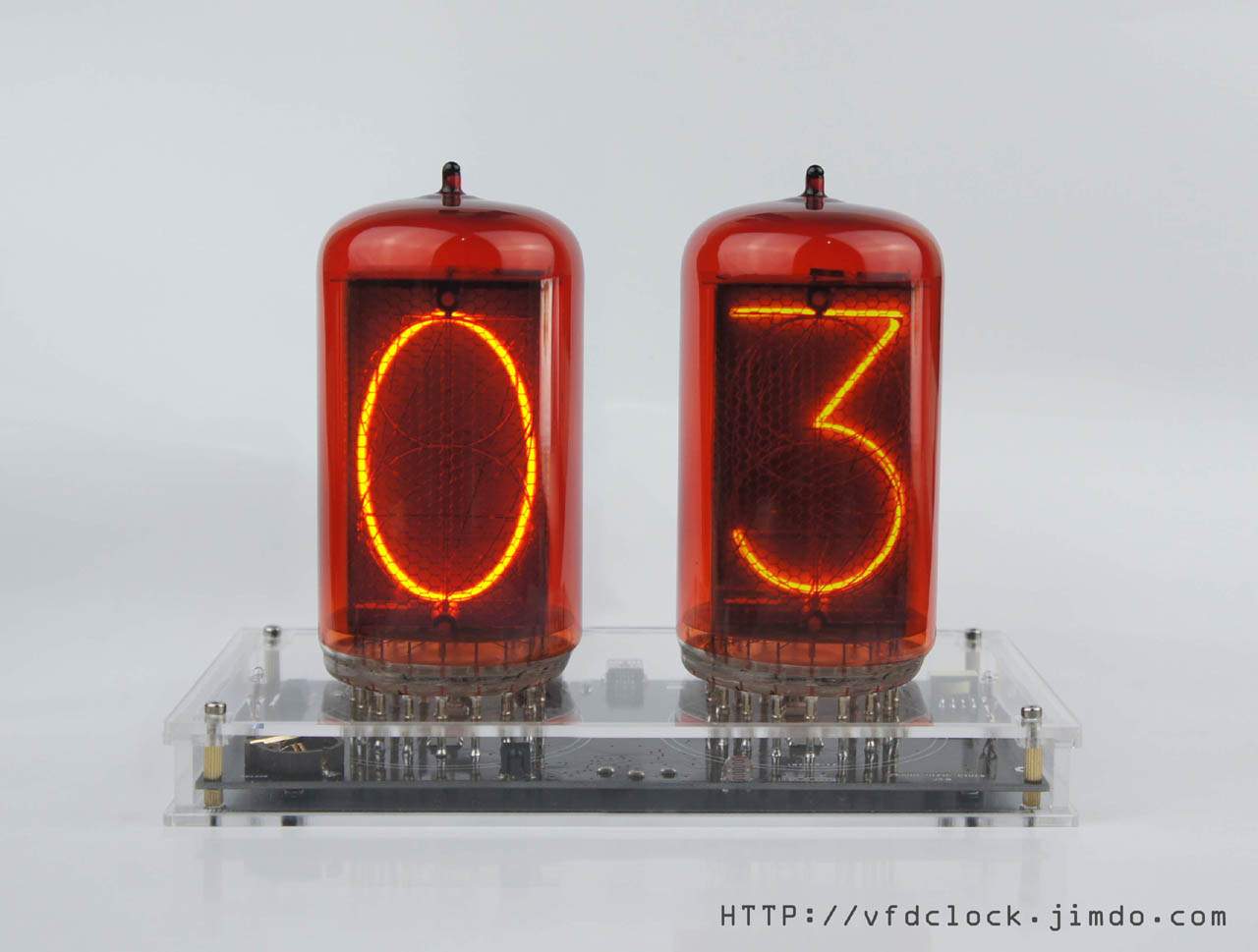
Product Change Notification in the New Version:
-------------------------------------------------------------------------------------------------------
Specifications:(For reference only)
Tube
Name: Z568M ;
Tube Size:50mm(dia.);
Tube Height:107mm;
Digit Height:50mm;
Clock Supply: 5V DC via USB;
Working Current: ~660mA;
Clock Size:156mm(L)*80mm(W)*18mm(H)-(*no including the tube);
PCB Size:146mm*70mm;
PCB Color: Black;
Weight:~280g(weight with the tube installed);
The clock works with any standard USB power supply,use only high-quality adapter!

Features:(For reference only)
You can replace the tube(s) by yourself without using any tools.
1). 5V USB powered,easy to be used. Can connect to your computer's USB plugs directly.
2). Support 12H or 24H display modes, can show "."as“A/P" in 12H time format.Leading zero blanking is programmable.
3). Display date in all format: YY.MM.DD or DD.MM.YY or MM.DD.YY or even MM.YY.DD.
4). Support different Effs:Normal/Fading/Cross Fading/Slow Fading/Loop for displaying time.
5). High accuracy DTCXO (temperature compensated crystal oscillator) inside,+-4.94 seconds(MAX) per month.
6). Simple setting by using 2 buttons only and supports IR remote control(optional).
7). Three alarms with weekends ON/OFF support,can be controlled individually.
8). Three programmable Auto Power ON/OFF mode,can turn ON/OFF NIXIE tubes in any time you want.This function can save tubes life.
9). 8-level adjustable NIXIE tube bright with Auto-brightness feature(its ability to adjust the tube
brightness depending on the current environment).
10). Rechargeable Backup Battery or Farad
capacitor keeps RTC running during power
outages.(May install a CR1220 battery socket instead if can't ship battery,please prepare 1pcs CR1220 battery by
yourself.)
(!!!RTC battery/cap keeps the real time clock running for a while after USB power
off,not keeping the whole clock running!!!)
11). Tri-colored RGB LED mounted under the NIXIE tube. These LEDs can display any color with a lot of predefined auto color change effects.
12). Store user settings in non-volatile memory.
13). Beautiful CAD designed acrylic case made using a laser cutter makes the clock look beautiful. You can assemble/disassemble the case by using only
4 screws on the bottom of the case.The case also has 4 bumpers as feet on the bottom of the case in order to stop to prevent case's damage.
14). Support temperature sensor(optional).

Tue
05
Feb
2019
DIP-USB Powered-Arduino 4-tube IN-12 NIXIE Clock-Open Source Code

Please use Acrobat Reader from ADOBE to open the PDF in the page,or you may not be able to get the attached files inside the PDF if using other PDF reader!!!

USB Powered 4-tube IN-12 NIXIE Clock-DIP version
DIP DIY KIT,Fully Open source, Arduino C code
This is my first USB Powered NIXIE 4-tube Clock design,the prototype has been working for over half year, works great.
We use Atmega328 MCU and DS3231 RTC in this design.
Features(for reference only):
1.Fully Fully open source code(ARDUNIO Source code in pure C);
2.DIP components, all smd equipments like DS3231 chip has been attached to a small PCB as a module,easy to assemble;
3.Plug-able design,we use female socket pins to install IN-12 NIXIE tubes, thus you can install NIXIE tubes by hand;
4.USB Powered, almost no heat when working;
5.All 0~9 segs in 4pcs IN-14 tubes can be light up;
6.Pure C Arduino source code, easy to understand, you can change the code by yourself or port to other platform if you wanna;
7.It has leds under NIXIE tubes, light it up or not depends on your own code;
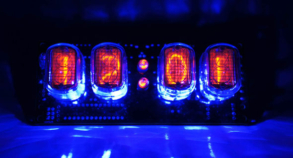
USB Powered
4-tube IN-12 NIXIE clock for ARDUINO
Assembly Instructions
V1.0
Notice
For assembling the NIXIE clock you need to have the skill of soldering DIP components. We use a Hakko FX-888 Soldering Station (with CF2 Iron Head). We use 183℃(degree C)low melt temperature solder wire S60, 0.5mm(Dia.), Brand Almit.
For how to solder the DIP components, we recommend:
https://www.hakko.com/english/tip_selection/type_bc_c.html
https://www.hakkousa.com/video/
Please do not change any equipments of the KIT or you may not be able to get the KIT
in working.
Because it contains no SMD components, so it is very easy for you to assemble, we recommend to check the circuit diagram carefully and follow the steps shown blow.
We do not recommend you to solder the components in random order or if it has problems you will need more time for de-soldering(*Will damage the PCB Pad) and debug, we recommend you follow the steps in this instructions that you can do part test after finished each step.
For more info & update, please visit HTTP://vfdclock.jimdo.com
Or contact us: zjjszhangf@gmail.com
Thanks for choosing our product.
Building it
Well, because of the circuit is block based and not very complicated, all you need to do is get all the components in the right position and make sure no short or no float before you plug the power in. We will show the soldering steps blow.
Preparing
1. Please print out the PCB installation diagram by yourself, the Circuit diagram is no need for soldering job, print it or not depends on you(Note: May only have the paper circuit diagram in the KIT with no digital version provide.);
2. Check all the components in the kit bag, make sure nothing is missing (You can do this on a A4 white copy paper);
3. We recommend using a soldering station and small soldering tip for soldering this kit (we use F2 or CF2 type tip). We recommend using ~180℃ type soldering tin for this job. Please do not use the high temperature soldering tin in this project or you will damage components or the PCB;
Step 1: USB Power In and HV part
Solder the [USB Power In] part next; This part contains a USB socket and Boost circuit.
For soldering the USB socket, we recommend solder the middle Pins first, then flip the PCB to the other side solder the two fixed side legs.
HV part is a SMD/DIP module,just solder on the pad,for SMD version,solder one pad first to locate the HV moudule,then solder the rest pads

Step 2: Solder the Electronic PINs for Neons and IC sockets
Recommend solder the Neons' PINS in the first place. You can plug the PINs on the top of the PCB then
cover a had board like a small PCB or small wood board over the PINs, use two clamps to hold it with the main PCB, then flip the PCB. Now you can solder on the other side.
3 parts pins, 2 in the middle of PCB as colon, the other one is for PM-dot.
IC sockes are easy,just take care of the first leg direction.
Tips: Because of the PINs are through hole version, please solder it carefully and do not let the tin goes in to the inside of the pins or will damage the PINs.
If necessary, you can plug a wood /bamboo toothpick in the PINs hole when soldering.
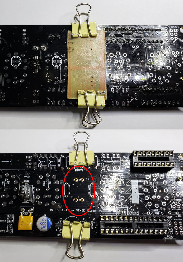
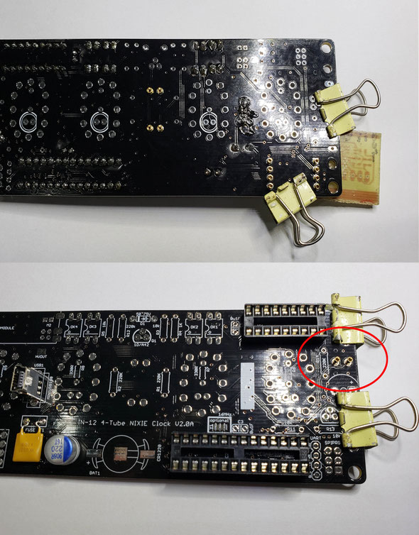
Step 3: HV module and HV lift part
In this step, you only need to solder one resistor and one diode and one HV supply module, usually the diode is the small glass one, the cathode side contains a black or others color mark, please do not go invert.
(And please use 1W resistor if you damaged the org one).
*The HV module may have different version and outlooks,like DIP version or SMD version,but in same function.
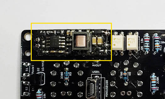

Step 4: OP(opto-coupler) Driver part
Now we can solder the OP driver part components. This part of the circuit contains 2pcs resistors (1k and 10k), and 4pcs of OP(optocoupler), just need to take care of the OP direction, do not go invert;
And because of the circuit connected to the High Voltage circuit, the 10K resistor in this part you need to use the big one(1/2w) resistor, do not use the small (1/6W or 1/8W) one, or the resistor will be damaged under high voltage and the circuit will not work stable;
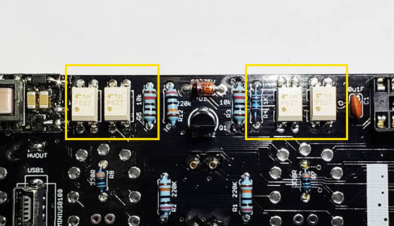
Step 5: Chips part and rest misc part
The Chips part contains 2pcs DIP chips;These 2 DIP chips can be installed directly or installed by using
the DIP socket(*May need to prepare the chip sockets by yourself!!!) depends on you. Please take care of the Chips
direction;

Step 6: LED part
The LED part contains 4pcs LEDs and 4pcs resistors; please note that the LED should be installed on the
top side of the PCB, and please solder the LED fast to prevent its be damaged;And please take care of the LEDs' direction, do not go invert(it contains one flat side);
The Led resistors may have different value for RED LED or Blue LED or others color LED, the RLED will be stored with the LEDs, usually the value is in 150R~330R range.

Step 7:NIXIE pins
Now we are going to solder the IN-12 PINS.Please flip the PCB to the front side,the PINS need to be installed on this side and please solder it on the middle part of the PINs;
First we recommend you plug the PINS in the IN-12 legs,then plug ALL the PINS to the install holds,plug it down to the middle part, then flip the PCB ,solder the PINs on the bottom side of PCB;

!!!Plase double check to see if all PINs are plugged to the middle part before you solder the PINs!!!

Step 7: First Testing
After finished all the steps shown up, please recheck it to see if has no error on PCB.
Now we can plug the USB power in, if all fine, the NIXIE tubes will display the time.
If has error, or the PCB did not work, please recheck the circuit block by block to see if it has any shot or float on PCB.
Step 8: Cleaning Circuit Board
You can use the household rubbing alcohol and a toothbrush to remove the solder flux on the PCB.
If available, the anhydrous alcohol (used for electronics cleaning) works much faster. Blot the cleaned area with a non-linting tissue (like Kimwipes EX-L) or a clean towel or you can do it in your own way.
Step 9: Buttons and Buzzer etc.
Because of Buttons and Buzzer etc. can not be washed, we need to solder 3pcs Keys and 1pcs Buzzer after cleaning the PCB.
Buzzer output part needs to face the outside of PCB, one long leg is [+] leg, do not go invert.
If the Buttons are one side two pins version,just solder it directly on PCB,if the Buttons are two side 4pins version,cut one side 2 pins off buy yourself,and band it flat the other side of 2pins then solder it and cut it short(or cut it short first before soldering);
Also do not forget to plug 2pcs neon bulbs in the female sockets as middle colon,and cut the rest of legs on the bottom side.
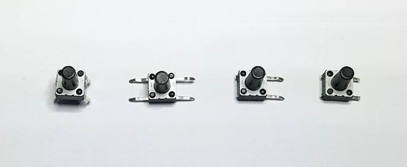
Step 9: Extras
There are UART and AVR SPI port has been designed on PCb, if you need to use these functions, solder PINs by yourself.(*Prepare STD. 1*4 PINs(UART) and(or) 2*3 Pins(SPI) by yourself.)
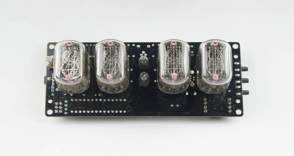

How to set time
After USB Power ON,the clock will display the time.
Now it is in the [Time display Mode] and there are 3 keys on the right side of the clock,[MODE],[+]and[-];
Single click the [MODE] key,will switch to [Set Hour mode], tubes will display [01:xx],then you can click the [+]/[-] key to adjust the current hour;
Single clock the [MODE] key again,will switch to [Set Minute mode], tubes will display [02:xx],then you can click the [+]/[-] key to adjust the current minutes;
Single clock the [MODE] key again,will switch to [Set Time Format mode], tubes will display [03:xx],then you can click the [+]/[-] key to adjust the current timne format like in 24/12hours mode,etc.;
Single clock the [MODE] key again,the clock will back to the [Time Display Mode];
----------------------------------------------------
When in [Time display Mode],if you click the [+] key can switch display in between HH:MM and MM:SS format,click [-] key can turn the LED ON/OFF;
Slotmachine eff will be triggered in every 10 mins automatically.
The password of the PDF will be attached inside the parcel.
Please use the Acrobat Reader from Adobe to open it and you can find the source in the attachment part of PDF.
Wed
11
Jul
2018
DIMMER-Ver Pluggable USB-Powered-IV-9(ИВ-9) 6-Tube NUMITRON Clock
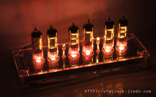
6t-nb-9
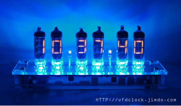
Notice
For indoor use only.
Specifications
(For
reference only)
Tube Name: IV-9(ИВ-9)(Made in the U.S.S.R.)
Tube Diameter: 11mm;
Tube Height: 35mm (no including the legs);
Symbol Height: 10mm;
Clock Supply: 5V DC via Mini/Micro USB;
Max Current: ~600mA;
Clock Size: ~124mm (L)*42mm(W)*12mm(H)(*~50mm(H)with tube(s) be installed);
PCB Size: 114mm*32mm;
PCB Color: Black/Green;
Weight: ~220g(with IV-9(ИВ-9) tubes);
The clock works with any standard 5V/1A USB supply, use only high-quality adapter!
Features
1).5V USB powered, easy to be used;
2).High efficiency circuit, circuit gets almost no heat under 24*7 working condition;
3).Pluggable design, Static driving, No Flashing, High Brightness;
4).Support 12H or 24H display modes. Leading zero blanking
is programmable.
5).Display date in all format: YY.MM.DD or DD.MM.YY or MM.DD.YY or even MM.YY.DD; Can display week info too.
6).Support a lot of different Effects: Normal/ Fading/ Cross Fading/Flash /Loop /Random Loop/ Scroll + Mix1/mix2 for displaying time (* Effects may will be changed in the future);
7).High accuracy RTC inside, DTCXO (temperature compensated crystal oscillator) version, High Stability, Highly accurate. It has ±1.9ppm (Equivalent to ±4.94s seconds of month deviation) under 0ºC~+40ºC. Usually you don't need to set the time
for over a year;
8).Simple setting by using 3 buttons only and supports IR remote control (optional). Also has a new SNOOZE button.
9).Three alarms with weekends ON/OFF support can be controlled individually.
10).Three programmable Auto Power ON/OFF mode, can turn ON/OFF NUMITRON tubes in any time you want. This function can save tubes life.
11).ML621 re-chargeable battery
on-board for the RTC power which keeps RTC running during power outages. (*May
install a battery socket only because of can not ship battery!)
13).Tri-colored RGB LED mounted under the each NUMITRON tube. These LED(s) can display pre-defined
auto color change effects.
14).Store user settings in non-volatile memory.
15).Beautiful CAD designed acrylic case made using a laser cutter makes the clock look beautiful;
16).Can install Temperature Sensor(optional);
18).8-level adjustable NUMITRON tube bright with Auto-brightness feature (it is able to adjust the tube
brightness depending on the current environment).
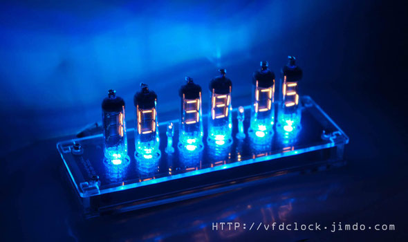
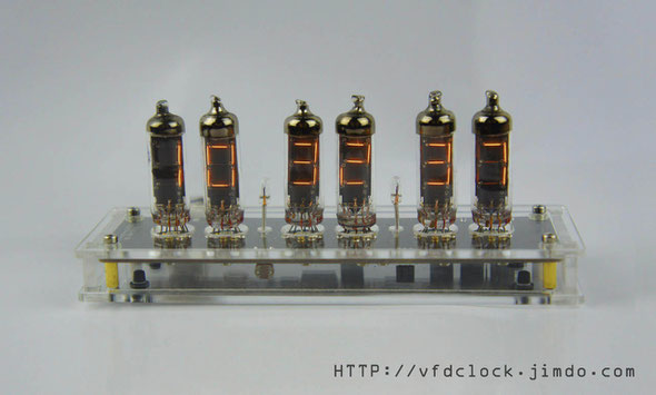
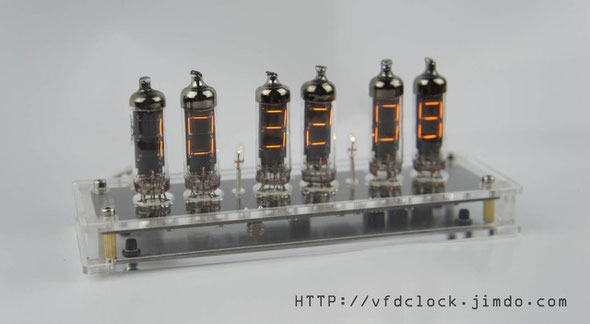
Wed
11
Jul
2018
DIMMER-Ver Pluggable USB-Powered-SZ-J2/QS27-1 6-Tube NIXIE Clock

NEW-V3.0 Dimmer version-Plug-gable - USB Powered SZ-J2/QS27 6-Tube Digit NIXIE Tube Clock.
This Plug-able SZ-J2/QS27-1 6-tube NIXIE clock can be placed horizontally or tilted with tilt-back legs installed(For easy to read the tubes on desktop).
All SZ-J2 NIXIE tubes and the middle neon
bulbs(colon) are installed via electronic PINs. You can replace the tubes and the middle colons by yourself by hand directly.
This type of NIXIE tube SZ-J2/QS27-1 has beautiful number [5],please check the
pics.
Product Change Notification in the New
Version:
1.It supports 8-level dimmer function for the SZ-J2/Qs27-1 NIXIE tubes with Auto-brightness feature(its ability to adjust the tube brightness depending on the current
environment);
USB Powered;Slim design;Almost no heat;Static driving;No Flashing;
Notice:
In order to drive the NIXIE tube, some internal
equipment is under the High Voltage,please do not use this clock outside or in any wet conditions,please do not touch any part inside the clock when power on.Always keep it away from kids.
Specifications(For reference only):
Tube Name:SZ-J2/QS27-1(Made in the P.R.C.);
Tube Size: (26mm(L)*20mm(W)*25mm(H)+7mm(H-pins)
)
Clock Supply: 5V DC via USB;
Current: ~600mA(MAX);
Power: ~3W;
Clock Size:198mm(L)*61mm(W)*22mm(H)(*~43mm(H)with SZ-J2/QS27-1 tubes installed);
PCB Size:186mm*55mm;
PCB Color: Black;
Weight:~192g;
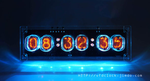
Features(For reference only):
1. USB 5V powered, easy to be used. Can connect to your computer's USB
plugs directly (* or use any 5V 1A or up USB power adapter).
2.High efficiency HV circuit, you got almost no heat in 24*7 working condition;
3.All SMT component, very thin PCB, Static driving, No Flashing, High Brightness
4.Support 12H or 24H display
modes. Leading zero blanking is programmable.
5.Display date in all format: YY.MM.DD or DD.MM.YY or MM.DD.YY or even MM.YY.DD; Can display week info too.
6.Support a lot of different Effects: Normal/Fading/Cross Fading/Flash /Loop/Random
Loop/Scroll in&out/Combine1/Combine2 for displaying time.(* Effects may will be changed in the future).
7.High accuracy RTC inside, DTCXO (temperature compensated crystal oscillator) version, High Stability, Highly accurate. It has ±1.9ppm (Equivalent to ±4.94s seconds of month
deviation) under 0ºC~+40ºC. Usually you don't need to set the time for over a year.
8.Simple setting by using 3 buttons only and supports IR remote control (optional).Also has a new [SNOOZE] button.
9.Three alarms with weekends ON/OFF support can be controlled individually.
10.Three programmable Auto Power ON/OFF mode, can turn ON/OFF NIXIE tubes in any time you want. This function can save tubes
life.
11.CR1220 battery socket on-board for the RTC power which
keeps RTC running during power outages. (*Prepare the CR1220 battery by yourself.)
12.Tri-colored RGB LED mounted under the each NIXIE tube. These LEDs can display different colors with pre-defined auto color change effects.
13.Store user settings in non-volatile memory.
14.CAD designed acrylic case made by using a laser cutter makes the clock look beautiful. You can assemble/disassemble the case by using only 4 screws on the bottom of the case. The case also has
2 tilt-back legs as feet on the bottom of the case to placed the clock tilted for easy to read the time on desktop.
15.Can install Temperature Sensor(optional) ;Can install 433M wireless module(optional) for receiving the outside info, like the wireless
temperature sensors' data and the GPS time sync data, etc.
16. 8-level adjustable NIXIE tube brightness with Auto-brightness feature(its ability to adjust the tube brightness depending on the current
environment);
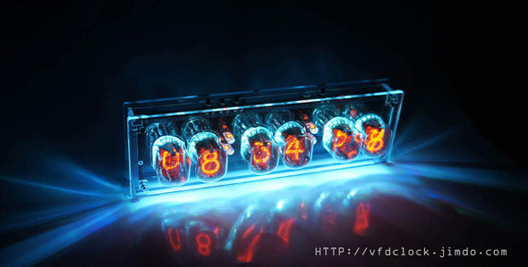
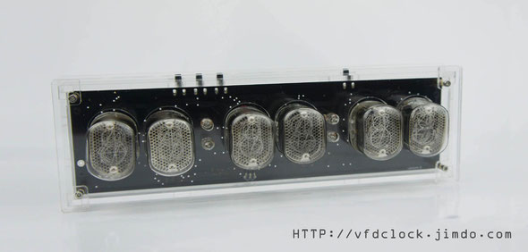
Wed
11
Jul
2018
DIMMER-Pluggable-USB-Powered-IV-11+IV-15 6-Tube VFD Clock Pro-V3.0-DIP

Specifications
(For
reference only)
Tube Name: IV-11(Made in the U.S.S.R.)
Tube Diameter: 22.5mm;
Tube Height: 60mm (no including the legs);
Digit Height: 21mm;
Digit Width: 14.6mm;
Clock Supply: 5V DC via Mini/Micro USB;
Max Current: ~600mA;
Clock Size: ~233.6mm (L)*66.6mm(W)*18mm(H)(*~81mm(H)with IV-11 tube installed);
PCB Size: 222mm*55mm;
PCB Color: Black;
Weight: 420g(with IV-11 tubes);
The clock works with any standard 5V/1A USB supply, use only high-quality adapter!
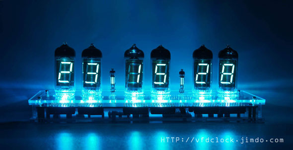
Features(For reference only)
1).5V USB powered, easy to be used;
2).High efficiency HV&LV circuit, you get almost no heat in HV&LV DC-DC part under 24*7 working condition;
3).DIP style design, Static driving,
No Flashing, High Brightness;
4).Support 12H or 24H display modes. Leading zero blanking is programmable.
5).Display date in all format: YY.MM.DD or DD.MM.YY or MM.DD.YY or even MM.YY.DD; Can display week info too.
6).Support a lot of different Effects: Normal/ Fading/ Cross Fading/Flash /Loop /Random Loop/ Scroll + Mix1/mix2 for displaying time (* Effects may will be changed in the future). All Effects support “SLOT MACHINE” effect except Mix1&Mix2;
7).High accuracy RTC inside, DTCXO (temperature compensated crystal oscillator) version, High Stability, Highly accurate. It has ±1.9ppm (Equivalent to ±4.94s seconds of month deviation) under 0ºC~+40ºC. Usually you don't need to set the time
for over a year;
8).Simple setting by using 3 buttons only and supports IR remote control (optional). Also has a new SNOOZE button.
9).Three alarms with weekends ON/OFF support can be controlled individually.
10).Three programmable Auto Power ON/OFF mode, can turn ON/OFF VFD tubes in any time you want. This function can save tubes life.
11).CR1220 battery socket on-board
for the RTC power which keeps RTC running during power outages. (*Prepare the
CR1220 battery by yourself.)
13).Tri-colored RGB LED mounted under the each VFD tube. These LED(s) can display pre-defined auto
color change effects.
14).Store user settings in non-volatile memory.
15).Beautiful CAD designed acrylic case made using a laser cutter makes the clock look beautiful;
16).Can install Temperature Sensor(optional);
17).Can Install PIR(Human Sensor Module) (optional) to turn the clock ON/OFF by detecting the human body;
18).8-level adjustable VFD tube bright with Auto-brightness feature (it is able to adjust the tube
brightness depending on the current environment).
19).Support Wireless GPS Module (optional), can sync time via wireless signal(*Need to have a GPS wireless time
station as time signal sender);


Sat
31
Mar
2018
B7971 Huge Single Digit NIXIE Tube Clock-Pluggable-USB Powered

Specifications:
Tube Name: B7971 ;
Tube Size:50mm(dia);
Tube Height:11.5mm(12.3mm with leg);
Digit Height:52mm;
Clock Supply: 5V DC via USB;
Working Current: ~260mA;
Clock Size:90mm(L)*80mm(W)*18mm(H)-(*no including the tube);
PCB Size:80mm*70mm;
PCB Color: Black;
Weight: 150g(weight with the tube installed);
The clock works with any standard USB power supply,use only high-quality adapter!
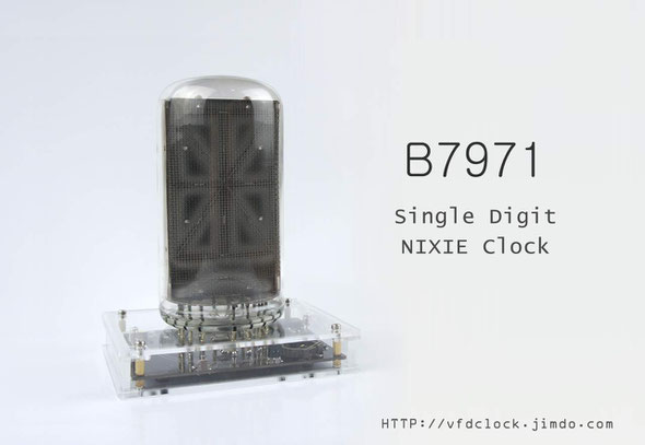
Features:
You can replace the tube by yourself without using any tools.
1). 5V USB powered,easy to be used. Can connect to your computer's USB plugs directly.
2). Support 12H or 24H display modes, can show "."as“A/P" in 12H time format.Leading zero blanking is programmable.
3). Display date in all format: YY.MM.DD or DD.MM.YY or MM.DD.YY or even MM.YY.DD.
4). Support different Effs:Normal/Fading/Cross Fading/Flashing/Loop for displaying time;Support 4 pre-defined Digit Fonts.
5). High accuracy DTCXO (temperature compensated crystal oscillator) inside,+-4.94 seconds(MAX) per month.
6). Simple setting by using 2 buttons only and supports IR remote control(optional).
7). Three alarms with weekends ON/OFF support,can be controlled individually.
8). Three programmable Auto Power ON/OFF mode,can turn ON/OFF NIXIE tubes in any time you want.This function can save tubes life.
9). 8-level adjustable NIXIE tube bright with Auto-brightness feature(its ability to adjust the tube brightness depending on the current environment).
10). Rechargeable Backup Battery or Farad capacitor keeps RTC running during power outages.
11). Tri-colored RGB LED mounted under the NIXIE tube. These LEDs can display any color with a lot of predefined auto color change effects.
12). Store user settings in non-volatile memory.
13). Beautiful CAD designed acrylic case made using a laser cutter makes the clock look beautiful. You can assemble/disassemble the case by using only 4 screws on the bottom of the case.The case
also has 4 bumpers as feet on the bottom of the case in order to stop to prevent case's damage.
14). Support temperature sensor(optional).
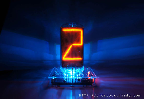

Sun
04
Mar
2018
Pluggable-IN-18 6-tube NIXIE clock fully assembled Version Ver.3.0

Notice
In order to drive the NIXIE tube, some internal equipment are under the High Voltage (up to ~180V DC), please do not use this clock outside or in any wet conditions, please do not touch any part inside the clock when power supply is turned on. Always keep it away from kids.
Specifications
(For
reference only)
Tube Name: IN-18(Made in the U.S.S.R.)
Tube Diameter: 30mm;
Tube Height: 68mm (no including the legs and the glass nipple);
Digit Height: 40mm;
Digit Width: 22mm;
Clock Supply: 12V DC via 5.5/2.1(or 2.5) Socket;
Max Current: ~850mA;
Clock Size: ~272mm (L)*72mm(W)*20mm(H)(*86mm(H)with IN-18 tube installed);
PCB Size: 260mm*60mm;
PCB Color: Black;
Weight: ~418g(with enclosure,with IN-18 tubes);
The clock works with any standard 12V-DC supply(5.5mm/2.1mm centre positive), use only high-quality adapter!

Features(For reference only)
1).12V DC powered with input reverse polarity protection on board, easy to be used;
2).High efficiency HV circuit, you get almost no heat in HV DC-DC part under 24*7 working condition;
3).DIP style design, Static driving, No
Flashing, High Brightness, No blue dots; Pluggable design all NIXIE tubes include middle commas are installed via
socket,can rplace by hand;
4).Support 12H or 24H display modes. Leading zero blanking is programmable.
5).Display date in all format: YY.MM.DD or DD.MM.YY or MM.DD.YY or even MM.YY.DD; Can display week info too.
6).Support a lot of different Effects: Normal/ Fading/ Cross Fading/Flash /Loop /Random Loop/ Scroll + Mix1/mix2 for displaying time (* Effects may will be
changed in the future). All Effects support “SLOT MACHINE” effect except Mix1&Mix2;
7).High accuracy RTC inside, DTCXO (temperature compensated crystal oscillator) version, High Stability, Highly accurate. It has ±1.9ppm (Equivalent to ±4.94s seconds of
month deviation) under 0ºC~+40ºC. Usually you don't need to set the time for over a year;
8).Simple setting by using 3 buttons only and supports IR remote control (optional). Also has a new SNOOZE
button.
9).Three alarms with weekends ON/OFF support can be controlled individually.
10).Three programmable Auto Power ON/OFF mode, can turn ON/OFF NIXIE tubes in any time you want. This function can save tubes life.
11).CR1220 battery socket on-board for the RTC power which
keeps RTC running during power outages. (*Prepare the CR1220 battery by yourself.)
13).Tri-colored RGB LED mounted under the each NIXIE tube. These LED(s) can display pre-defined
auto color change effects.
14).Store user settings in non-volatile memory.
15).Beautiful CAD designed acrylic case made using a laser cutter makes the clock look beautiful;
16).Can install Temperature Sensor(optional);
17).Can Install PIR(Human Sensor Module) (optional) to turn the clock ON/OFF by detecting the human body;
18).8-level adjustable NIXIE tube bright with Auto-brightness feature (it is able to adjust the tube
brightness depending on the current environment).
19).Support Wireless GPS Module (optional), can sync time via wireless signal(*Need to have a GPS wireless time
station as time signal sender);
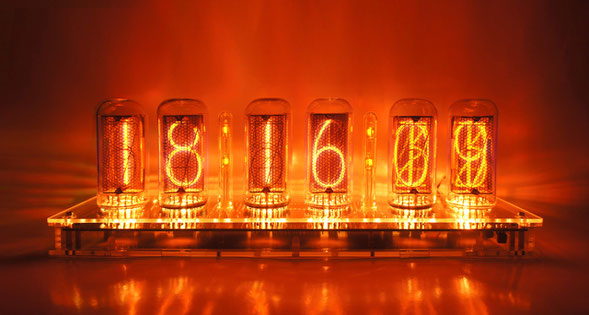
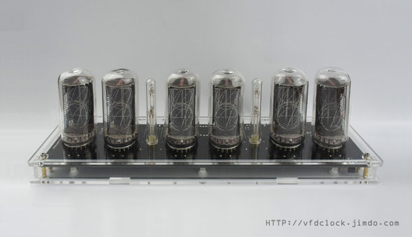
Sat
10
Feb
2018
DIY DIP KIT-Pluggable IN-18 6-tube NIXIE clock-Open Hardware
This is a 100% fully open hardware circuit(with the MCU main board circuit), IN-18 6-tube NIXIE clock DIY kit by using DIP components.
Because of hard to find the MCU that we are using in DIP package,we created a PCB,it converts the SMD MCU to DIP-SOW module,thus you do not need to solder SMD MCU, the module has been fully assembled and tested.
It costs us over two years time and 7 versions of PCB design.
All plug-gable design,all the IN-18 tubes and middle comma dots are all plug-gable,you can replace the NIXIE tubes and middle commas by hand.
And the Main MCU board and NIXIE driver Chips are all plug-gable on the PCB.
In Current Version we have moved all the equipment to the bottom of the PCB. It only has Female socket PINs and LEDs on the TOP of the PCB.
All the info shown blow is for reference only,we may change the circuit and PCB etc. without notification!!!
DIP-IN-18 6-tube Clock DIY version
Assembly Instructions
V1.0
Notice
For assembling the NIXIE KIT you need to have the skill of soldering DIP components. We use a Hakko FX-888 Soldering Station (with CF2 Iron Head). We use 183℃(degree C)low melt temperature solder
wire S60, 0.5mm(Dia.), Brand Almit.
For how to solder the DIP components, we recommend:
https://www.hakko.com/english/tip_selection/type_bc_c.html
https://www.hakkousa.com/video/
Please do not change any equipments of the KIT or you may not be able to get the KIT in working.
Because it left almost no SMD components(The only one is big MOSFET may in SMD package), so it is very easy for you to assemble, we recommend to check the circuit diagram carefully and follow the
steps shown blow.
We do not recommend you to solder the components in random order or if it has problems you will need more time for de-soldering(*Will damage the PCB Pad) and debug, we recommend you follow the steps in this instructions that you can do part test after finished each step.
For more info & update, please visit HTTP://vfdclock.jimdo.com
Or contact us: zjjszhangf@gmail.com
Thanks for choosing our product.
Building it
Well, because of the circuit is block based and not very complicated, all you need to do is get all the components in the right position and make sure no short or no float before you plug the
power in. We will show the soldering steps blow.
Preparing
1. Please print out the PCB installation diagram by yourself, the Circuit diagram is no need for soldering job, print it or not depends on you(Note: May only have the paper circuit diagram in the
KIT with no digital version provide.);
2. Check all the components in the kit bag, make sure nothing is missing (You can do this on a A4 white copy paper);
3. We recommend using a soldering station and small soldering tip for soldering this kit (we use F2 or CF2 type tip). We recommend using ~180℃ type soldering tin for this job. Please do not use
the high temperature soldering tin in this project or you will damage components or the PCB;
Please always remember that in this new version,only LEDs and NIXIE PINS and comma PINs are installing on the TOP side of PCB,others are all on the bottom side of PCB.
And double check the component before you solder it on PCB, and also double check its' direction for some diode and caps etc.,DO not go wrong,because of if go wrong,de-soldering DIP component is not very easy, may damage the PCB pad.
Step (1): 12VPower In and 5V Power Out
Solder the [Power In&12V->5V] part first; This part contains a 5.5/2.1 12V power in socket and 12V->5V circuit.
This part is easy,it contains a 5.5/2.1 12V in socket,a fuse,a diode,and a typical 7805 12V-5V convert circuit which contains a 7805 chip and two caps.
For the diode, please check the direction carefully, the cathode side contains a white mark.
Also take care of the C5 and C6(Aluminum Electrolytic Capacitor), it has polarity, do not install it in invert direction;
After soldering this part,you can plug the 12V in,then measure to see if the C6 has 5V output;

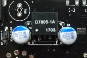
Tips:
The 7805 works fine in this design, if wanna get higher efficiency of the 12V->5V part,you can use some 12V->5V 3pin DC-DC module to replace 7805 Chip(Like the D7805 in the pic).
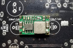
In some of versions,we also designed an optional DC-DC module install pins on the PCB for easy to replace the regular 7805 circuit;
If have this DC-DC version of KIT,just need to solder the 12V->5V DC-DC module on the PCB, and no need to solder the two in&out capacitors, because of caps are already on the module;
Step (2): Middle comma Pins and MCU IC socket pins
We need to solder some pins in this step,please solder it in this step,will be easier to be installed.
The first PINS are middle comma female pins,please plug the Female PINs on the top of the PCB then cover a had board like a small PCB or
small wood board etc.over the PINs, use two clamps to hold it with the main PCB, then flip the PCB. Now you can solder on the other side.
Tips: Because of the PINs are through hole version, please solder it carefully and do not let the tin goes in to the inside of the pins or will damage the PINs. If necessary, you can plug a
wood/bamboo toothpick in the bottom of PINs hole when soldering.

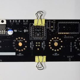

Then solder the MCU IC sockt on the bottom of the PCB,this part is easy,just plug the IC socket in the PCB,flip it and press it on the table,then solder it. Please take care of the direction of the IC socket(check the first leg mark of the socket), do not go invert and do not go wrong PCB side.
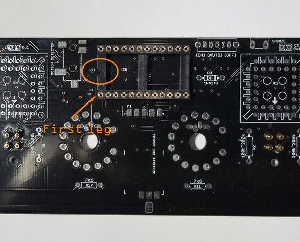
Step (3): Install LEDs
The LED part contains 6pcs LEDs(With Chip inside it) and 6pcs 0uF(100nF) caps; Please note that the LED should be installed on the top side of the PCB, and take care of the first leg of the LED(The first leg is on the FLAT side of LED, and the LED pad has a white [.] and flat line to point out the first leg on PCB); Please solder the LED fast to prevent its be damaged;
The LED legs are very close,please solder carefully. Do not short any legs.
After soldering one LED,we recommend you plug the power on to give it a test,make sure it works before install the next LED.(Remember to plug the MCU module when you test LED(s));
Do not forget to solder the 0u1(100nF) capacitor(s) near LEDs in this part on the bottom of PCB,and cut the legs as short as it can be installed;
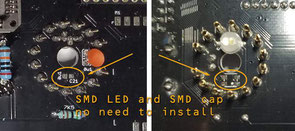
Notice:
In some of the PCB may contain a serial of SMD version of LEDs' pad in front of the PCB,these are for SMD version of LEDs and also has 0603 100nf caps on the back side of PCB, no need to install in DIP version,just ignore it.


We have sent the first 10PCS test KIT for the NIXIE DIY fans in the world, the returning info shows that they felt soldering the LEDs is the hardest part in this KIT, because of LED is heat sensitive component and the PINs are very close, easy to get short when do soldering. To solve this problem, we have improved the LED PAD design and add soldering tips blow for you to check.
Tips for soldering LED:
First plug the LED in the install place on the TOP of PCB(double check the direction, do not go invert),and use a PCB/Wood-Board etc.(like 1.6mm thick one) on one edge side of LED, it lifts the LED up a little bit,then you can plug a cotton applicator with alcohol on the other side,then flip the PCB,and solder all the LED legs.
Please do not cut the LED legs before soldering,if cut it short first, legs will be easy to short in soldering.
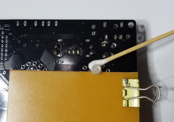
Soldering led legs tips:
We have improved the LED PAD into offset pad design, one side is longer than the other side for easy soldering. We recommend put the iron head on the longer pad to heat it up first then put the tin wire on the other side.
Soldering the left and right legs are easy, please solder these two legs first to fasten the LED, the hardest part is soldering the middle two PINs, may get short in this kind of small distance. We recommend use aluminium foil to cover the other legs first, then solder the middle legs one by one in between.(Check the Pics shown blow)
After soldering all legs, you need to double check to see if have any problems, if all fine, you can cut the legs in short.
If have any short, please use desoldering wick to solve the problem.
Always remember to solder the LED legs fast or will damage the LED!!!
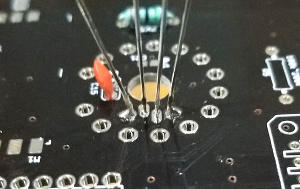
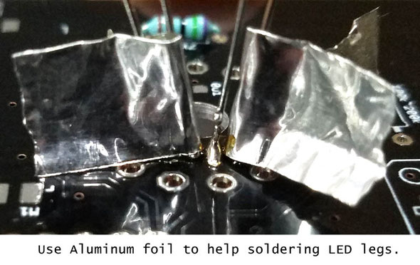
Step (4): HV part
The HV part is the major part of the design,it converts 12V to 165~170V high voltage,please take care of this part, do not get electric shock.
Please take care of the directions of diodes and Aluminum Electrolytic Capacitors in this part, do not go invert. And the mosfet Q4 is in SMD package, do not forget to solder the big pad on the top of the mosfet!!!
Do not forget the small glass diode D3 on the left side;
This part of the circuit contains two Jumpers,[VIN] for 12Vin, and [HVOUT] for HV output, remember to solder these two jumpers close. We design these two jumpers for easy to separate the HV part
circuit from other circuits, easy for debuging;
After soldering all component(* Do not go power on if only solder part of the components of this circuit or the HV output will lost control and damage
things!!!) in this part of circuit, and double check, then you can plug the 12V in. If the circuit in working, you will get about 165V~170V output between the two legs of the C3 HV output
capacitor;
The HV output cap. and Inductor need to be installed in 90 degree as shown in the pic blow;
Tips:
For the safety, recommend do not use any socket in the HV part of the circuit,and solder everything carefully in this part.
If the HV part did not work,please double check and fix the problem,do not do the next step if this step in no working!!!
Do not touch any part of the HV part when power on!!!

Notice:
For the two C8 and C9 input Aluminum Electrolytic Capacitors in this part, may only have one big Aluminum Electrolytic Capacitor in the kit,in this situation you can solder the big one in 90 degree way as pic shown blow.
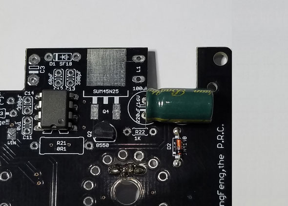
Step (5): PLCC sockets and misc Resistors and Caps etc.
This part is has two PLCC sockets,just plug the socket in the right direction(Please check the pic blow) then solder on the other side of the PCB.
Remember to solder two 0u1(100nF) caps in this part;
Also remember to solder 6pcs 7k5 IN-18 resistors and 4pcs resistors for middle commas;
And one CR1220 battery socket on the right side of the PCB ,near 7805 part,take care of direction.
And CDS and IR receiver(Optional) on the front side of the PCB;
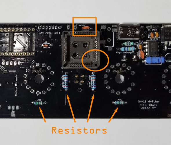
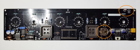
After finishing this part,about 80% of the PCB soldering job has done.
Step (6): IN-18 PINS
Now we are going to solder the IN-18 PINS.Please flip the PCB to the front side,the PINS need to be installed on this side and please solder it on the middle part of the PINs;
First we recommend you plug the PINS in the IN-18 legs,then plug ALL the PINS to the install holds,plug it down to the middle part, then flip the PCB ,solder the PINs on the bottom side of PCB;
!!!Plase double check to see if all PINs are plugged to the middle part before you solder the PINs!!!
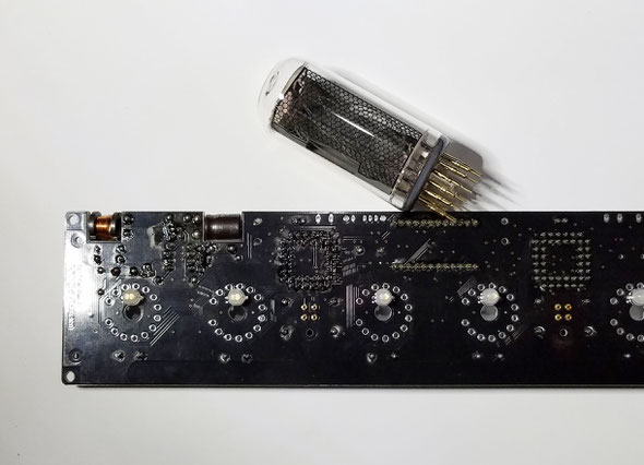
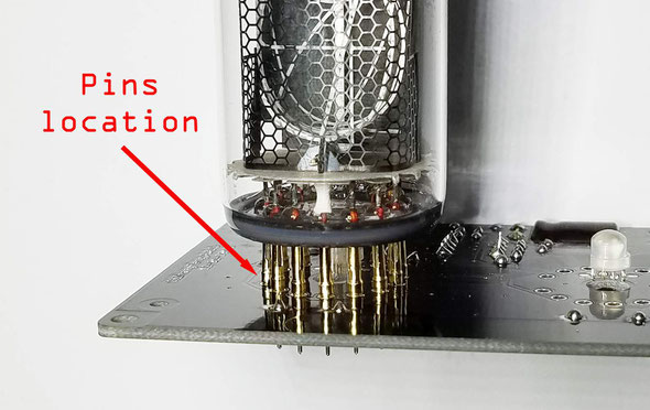
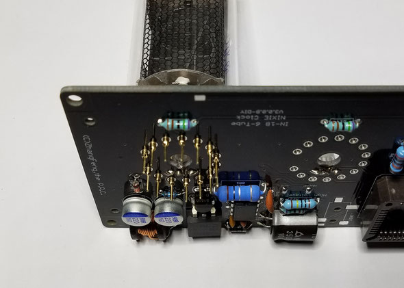
In soldering the PINS,if necessary,you need to keep pushing the tubes down to make sure all the PINS have been soldered on the middle part, please trade care of this part.
!!!Pleas note, do not add too much tin in soldering PINs,and please solder it fast. If add to much tin, the tin may go inside of the PINs and will solder the IN-18 tube legs with the socket,which will be big problem. We recommend add a little bit body lotion or oil on the surface of all in-18 PINs, will help to prevent be soldered together with socket.
And after finished soldering on tube PINS,give it a power on test(*Remember to plug the MCU module and HV driver Chips in socket for testing) to see if have any problem. If all ok, move to the next tube location;

After soldering and testing,if all fine,you can cut the thin part of PINS under the PCB if you want to or just leave it uncut depends on you.
We recommend cut it off,because the end of legs is soft, may cause short.

Step (7): Power ON Test
After finished all the steps shown up, please recheck it to see if has errors on the PCB.
Then plug the two PLCC HV driver Chips and Main MCU module in the sockets; please double check the direction of IC and module before power
on, do not go wrong direction.
Now we can plug the 12V power in, if all fine, the NIXIE tubes will display the time.We recommend plug one NIXIE tube in when in the first time power on test, if first NIXIE tube works, you can
go power off and add another one, do test again...etc., until all 6 tubes are all in working;
If find errors or the the clock did not work, please go power off and re-check the circuit block by block to see if it has any short or float on PCB;
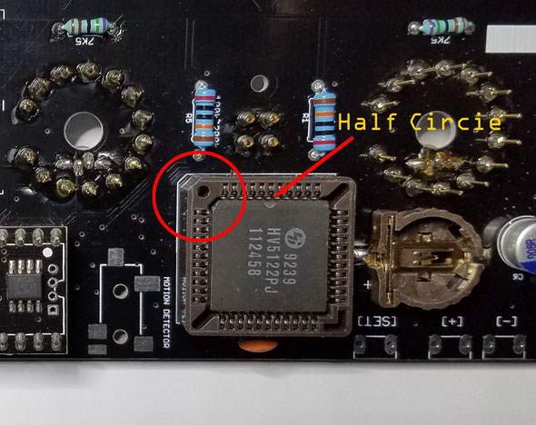

Step (8): Cleaning the Circuit Board
You can use the household rubbing alcohol and a toothbrush to remove the solder flux on the PCB.
If available, the anhydrous alcohol (used for electronics cleaning) works much faster. Blot the cleaned area with a non-linting tissue (like Kimwipes EX-L) or a clean towel or you can do it in your own way.
!!!Remember to remove the HV driver Chips and the MCU main board when cleaning the PCB!!!
You need to have a PLCC EXTRACTOR for unpluging the PLCC chip from the socket;
Step (9): Buttons and Buzzer etc.
Because of Buttons and Buzzer etc. can not be washed, we need to solder 4pcs Keys and 1pcs Buzzer after cleaning the PCB.
If the Buttons are one side two pins version,just solder it directly on PCB,if the Buttons are two side 4pins version,cut one side 2 pins off buy yoursele,and band it flat the other side of 2pins then solder it and cut it short(or cut it short first before soldering);
It also has two 3.5mm plug socket,one is for GPS, the other is for "PIR Motion Sensor";Please remember to solder these on PCB too;
And do not forget to solder the 3-brand switch (If has, some version may move this switch to the PIR sensor side) for the "PIR Motion Sensor",and remember to switch it to "ON/Auto" not "OFF" part to prevent it turns the HV output OFF when in the testing;
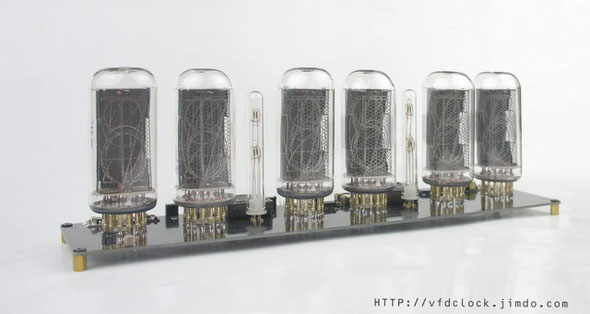
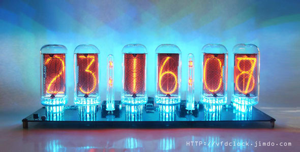
Extras (10): Create middle comma
For how to assembling the Middle comma,please visit:
KIT-Create the Middle Dot Comma for IN-18 NIXIE clock
You can make your own decision of the location of the bulbs in the middle glass tube.
Extras (10): misc extras
In editing...
test
In editing
Thu
03
Aug
2017
DIY KIT-USB Power-HV5W-E DC-DC module for NIXIE clock
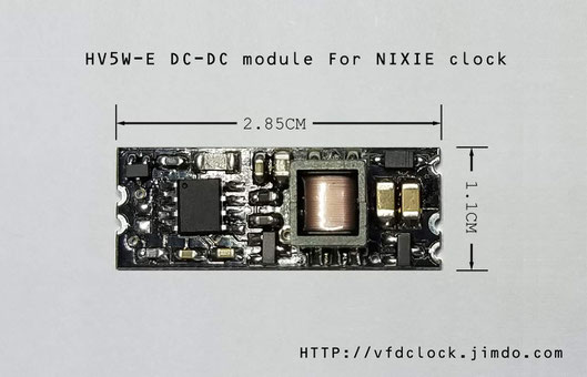
If have any questions ,you can contact us: zjjszhangf@gmail.com
And you need to have SMD soldering skill to assemble this KIT!
The newest design:
Vin=3V3~12V;
Vout= max 200V adjustable output;
(Add an extern resistor on PCB or connect outside the module for adjusting.)
En Pin for turning the Module On or OFF with 3V3, 5V or even 12V Logic signal range;
Std. 0.1# gap of PINS,you can install it on PCB as a small height SMD module;
Small Size, 2.85Cm*1.1Cm*0.55Cm(H), can light up 6~8pcs IN-12(IN-14) or 3pcs IN-18 at the same time with 3.7V Li battery or 5V USB power,you get almost no heat for 24*7 working condition;
For the people who can solder the SMD components, will have a KIT version for you to assemble the module by yourself.
For the assembly Instructions,check blow.
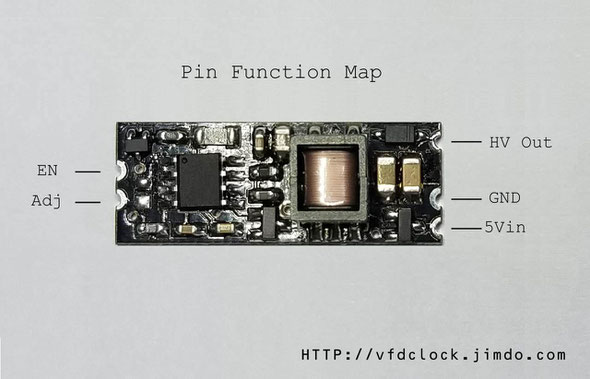
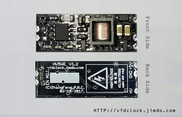
HV5W-E USB Powered
DC-DC HV Module for NIXIE Clock
Assembly Instructions
V1.0

zjjszhangf@gmail.com
HTTP://vfdclock.jimdo.com
Notice
For assembling the HV5W-E clock you need to have the skill of soldering SMD components. We use a Hakko FX-888 Soldering Station (with CF2 Iron Head) and a Hot air blower station. We use 183℃(degree C)low melt temperature solder wire S60, 0.5mm(Dia.), Brand Almit.
For how to solder the SMD components, we recommend:
https://www.hakko.com/english/tip_selection/type_bc_c.html
https://www.hakkousa.com/video/
Please do not change any equipments of the KIT or you may not be able to get the module working.
If already have the skill of soldering the SMD components, it is easy for you to assemble the KIT, please check the circuit diagram carefully and follow the steps shown blow.
Because of this module is small size module and contains few components, if you solder it carefully, it is very easy to be assembled, and no need debug. Please solder all the components and double check it before power on test.
For more info & update, please visit
HTTP://vfdclock.jimdo.com
Or contact us: zjjszhangf@gmail.com
Thanks for choosing our product.

Preparing
1. Please print out the PCB installation diagram by yourself, the Circuit diagram is no need for soldering job, print it or not depends on you(Note: May only have the paper circuit diagram in the KIT with no digital version provide.);
2. Check all the components in the kit bag, make sure nothing is missing (You can do this on a A4 white copy paper);
3. We recommend using a soldering station and small soldering tip for soldering this kit (we use F2 or CF2 type tip). If you have a hot air gun(or Hot air blower station) tool for soldering, that will be great. We recommend using ~180℃ type soldering tin for this job. Please do not use the high temperature soldering tin in this project, you may damage a lot of SMD components or the PCB;
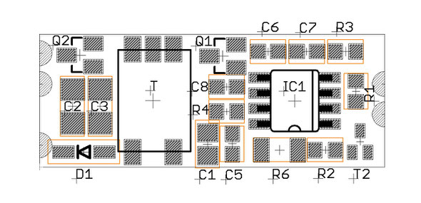
Identifying the parts of your kit
The following guide should help you to identify the parts and assemble it successfully.
Well, because of the circuit is very simple, we recommend you solder the main SO8 driver chip first, please double check it's direction, do not go invert.
Then solder all the capacitors, please control the temperature or the capacitor will be damaged.
The 0603 caps have two types (1uf and 1nf), please check carefully;
and 1 PCS 0805 size capacitor is 47uF/25V;
it also has 2 PCS 1206 big size capacitors are 1uF/250V; This 1206 type of capacitors are connected in parallel, we recommend you solder one only before debugging. Because if the output HV lost control when in the first power on test, you just damage one output cap not two.
Most of the resistors are also in 0603(or 0805) small size; The [R1] resistor is optional, if just manna create a constant out put 165V module for nixie clock instead of the output adjustable module, you do not need to solder this resistor.
and 1 PCS 1206 big size resistor is 1M;
All the resistors have the mark on its' surface, please check it before you solder it on PCB.
The triodes are easy, please take care of ESD free, and check the marks on its' surface.
The only one diode is [D1/E1J], it needs to take care of the direction, do not solder it invert.
The transformer has 2-3 pins structure, will not go invert.but you need to take care of it ,because of the magnetic core is easy to be crashed when dropping.
Tue
01
Aug
2017
DIP-USB Powered-Arduino NIXIE Thermometer-Open Hardware
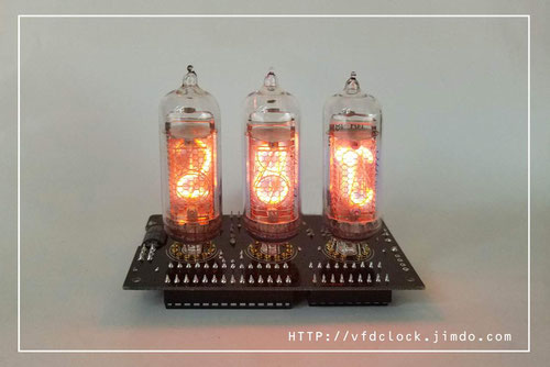
You can find the password of PDF inside the KIT BOX.
Please use Acrobat Reader from ADOBE to open the PDF in the page,or you may not be able to get the attached files inside the PDF if using other PDF reader!!!
USB Powered NIXIE Thermometer-DIP version-IN-14+IN-19
Fully Open Hardware, Fully Open source, Arduino C code
This is my first USB Powered NIXIE Thermometer design,the prototype has been working for about half year, works great.
We use Atmega328 MCU and DS18B20 sensor in this design.
Features(for reference only):
1.Fully open hardware+Fully open source code(ARDUNIO Source code in pure C);
2.Fully DIP components ,easy to assemble;
3.You can solder the NIXIE tube on the PCB directly or update to the plug-able version which you can just solder the female socket pins on the PCB first then
Plug the NIXIE tubes on it by hand;
4.USB Powered, almost no heat when working;
5.All 0~9 segs in 2 IN-14 tubes can be light up, and all segs in the IN-19 tubes can be light up too;
6.Pure C Arduino source code, easy to understand, you can change the code by yourself or port to other platform if you wanna;
7.It has leds under 3 NIXIE tubes, light it up or not depends on your own code;
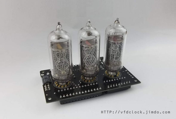
USB Powered
IN-14 + IN-19 NIXIE thermometer for ARDUINO
Assembly Instructions
V1.0
Notice
For assembling the NIXIE thermometer you need to have the skill of soldering DIP components. We use a Hakko FX-888 Soldering Station (with CF2 Iron Head). We use 183℃(degree C)low melt temperature solder wire S60, 0.5mm(Dia.), Brand Almit.
For how to solder the DIP components, we recommend:
https://www.hakko.com/english/tip_selection/type_bc_c.html
https://www.hakkousa.com/video/
Please do not change any equipments of the KIT or you may not be able to get the KIT in
working.
Because it contains no SMD components, so it is very easy for you to assemble, we recommend to check the circuit diagram carefully and follow the steps shown blow.
We do not recommend you to solder the components in random order or if it has problems you will need more time for de-soldering(*Will damage the PCB Pad) and debug, we recommend you follow the steps in this instructions that you can do part test after finished each step.
For more info & update, please visit HTTP://vfdclock.jimdo.com
Or contact us: zjjszhangf@gmail.com
Thanks for choosing our product.
Building it
Well, because of the circuit is block based and not very complicated, all you need to do is get all the components in the right position and make sure no short or no float before you plug the power in. We will show the soldering steps blow.
Preparing
1. Please print out the PCB installation diagram by yourself, the Circuit diagram is no need for soldering job, print it or not depends on you(Note: May only have the paper circuit diagram in the KIT with no digital version provide.);
2. Check all the components in the kit bag, make sure nothing is missing (You can do this on a A4 white copy paper);
3. We recommend using a soldering station and small soldering tip for soldering this kit (we use F2 or CF2 type tip). We recommend using ~180℃ type soldering tin for this job. Please do not use the high temperature soldering tin in this project or you will damage components or the PCB;
Step 1: Solder the Electronic PINs for NIXIE
(*If not the plug-able version, please skip this step)
For the Plug-able version, please solder the PINS in the first place. You can plug the PINs on the top
of the PCB then cover a had board like a small PCB or small wood board over the PINs, use two clamps to hold it with the main PCB, then flip the PCB. Now you can solder on the other side.
Tips: Because of the PINs are through hole version, please solder it carefully and do not let the tin goes in to the inside of the pins or will damage the PINs.
If necessary, you can plug a wood /bamboo toothpick in the PINs hole when soldering.
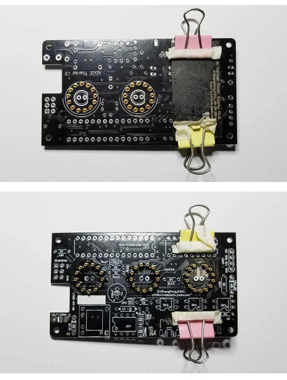
Step 2: USB Power In and HV part
Solder the [USB Power In] part next; This part contains a USB socket and Boost circuit.
For soldering the USB socket, we recommend solder the middle Pins first, then flip the PCB to the other side solder the two fixed side legs.
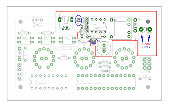
Then solder the Boost circuit part, it contains a DIP8 chip (We recommend solder it directly on PCB, do not use Chip Socket, because of if the Chip pins do not touch very well in the socket,the HV output may lost control).
Other Resistors and Capacitors are easy cake, for the diode, please check the direction carefully, the cathode side contains a black or white mark.
Also take care of the C1 and C2(Aluminum Electrolytic Capacitor), it has polarity, do not install it in
invert direction;
Especially for Aluminum Electrolytic Capacitor cap,usually it contains a white(or other
color long brand to mark the NEG(GND) pin on it's surface),this NEG(GND) pin needs to be plugged in the full-filled squire side of the mark on the PCB cap mark!!! Thus IN this case,C2 white marked side should be installed on the out-edge side of the PCB!
This part of the circuit contains two Jumpers ,JP1 for 5Vin, and JP2 for HV output, remember to solder these two jumpers close. We designed these two jumpers for easy to separate the HV part circuit from other circuits, easy for debugging;
After soldering all components(* Do not go power on if only solder part of the components of this circuit or the HV output will lost control and damage components!!!) in these circuit, and double check it, then you can plug the USB 5V in. If the circuit in working, you can find about 170V output in the two side of the C2 capacitor;

Step 3: HV lift part
In this step, you only need to solder one resistor and one diode, usually the diode is the small glass one, the cathode side contains a black or others color mark, please do not go invert.
(*Please note that the value of the resistor in this part is:
220K if using the HV6810 Chip in KIT;
100K if using the ST6810/16810 Chip in KIT;
And please use 1W resistor if you damaged the org one).
After soldering this part, you can measure the voltage of this part, it will have about 50V~75V range voltage between the glass diode;

Step 4: OP(optocoupler) Driver part
Now we can solder the OP driver part components. This part of the circuit contains 2pcs resistors (1k and 10k), and 3pcs of OP(optocoupler), just need to take care of the OP direction, do not go invert;
And because of the circuit connected to the High Voltage circuit, the 10K resistor in this part you need to use the big one(1/2w) resistor, do not use the small (1/6W or 1/8W) one, or the resistor will be damaged under high voltage and the circuit will not work stable;
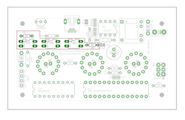
Step 5: Chips part
The Chips part contains 2pcs DIP chips + 1pcs DS18B20 sensor chip and 2 resistors and 1 capacitor;
The 2 DIP chips can be installed directly or installed by using the DIP socket(*May need to prepare the chip sockets by yourself!!!) depends on you. Please take care of the Chips direction;
Tips: For the DS18B20 sensor we recommend you keep the legs uncut and after soldering it on the PCB, you can band it into 90 degree position;

Step 6: LED part
The LED part contains 3pcs LEDs and 3pcs resistors; please note that the LED should be installed on the
top side of the PCB, and please solder the LED fast to prevent its be damaged;
The Led resistors may have different value for RED LED or Blue LED or others color LED, the RLED will be stored with the LEDs, usually the value is in 150R~330R range.
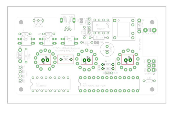
Step 7: NIXIE tubes part
For none plug-able version, you do need to solder the NIXIE tubes on the PCB; Before you solder the NIXIE tubes on, we recommend you test the LEDs first to see if it works fine.
In soldering the NIXIE tubes, we recommend you solder one or two legs of tube first, then you can adjust the tubes location ,make sure the tube has been installed vertically then you can solder the rest legs;
And please note the IN-14 tubes' anode pin should be plugged to the back middle hole as shown in the picture, usually for the IN-14&IN-19 NIXIE tube, the part of anode pin inside the NIXIE tube contains a white socket, easy to find out, and for IN-19 NIXIE tube, you will also find a short legs in front of the tube which is useless, you need to cut it off before you solder the tube on the PCB. And for IN-19 tube, you also need to expands the legs a little bit wide for easy to plug it in the PCB;
For plug-able version, you can just cut the legs in about 1cm length, then you can plug the tube in the socket which has been installed in the 1st step. For IN-19 tube, also need to cut the front short leg and expand all of the rest legs a little bit for easy to plug in; We recommend using sharp scissors to cut the legs into 45 degree sharp end, that will be easy for you to plug the tubes in the socket;
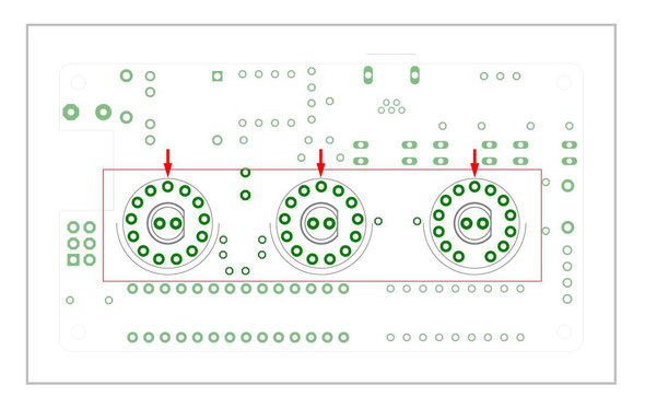
Step 7: First Testing
After finished all the steps shown up, please recheck it to see if has no error on PCB.
Now we can plug the USB power in, if all fine, the NIXIE tubes will display the temperature after self testing.
If has error, or the PCB did not work, please recheck the circuit block by block to see if it has any shot or float on PCB.

Step 8: Cleaning Circuit Board
You can use the household rubbing alcohol and a toothbrush to remove the solder flux on the PCB.
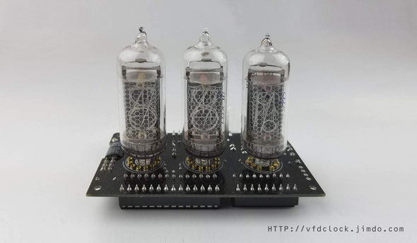
If available, the anhydrous alcohol (used for electronics cleaning) works much faster. Blot the cleaned area with a non-linting tissue (like Kimwipes EX-L) or a clean towel or you can do it in your own way.
update code
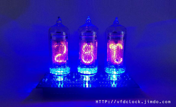
Step 9: Extras
There are UART and AVR SPI port has been designed on PCb, if you need to use these functions, solder PINs by yourself.(*Prepare STD. 1*4 PINs(UART) and(or) 2*3 Pins(SPI) by yourself.)
Add-ons:
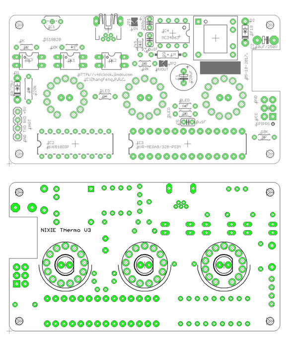

Tue
02
May
2017
AOTOM 20070-1A04 VFD Module for Arduino /AVR/PIC/STM/ARM/PI 5V ready


Specifications(For reference only):
Panel Name: AOTOM 20070-1A04
Panel Size: 70 mm*20mm;
Panel Color: Green;
Digit Height: 6.5 mm;
Supply: 5V DC;
Max Current: ~150 mA;
Module Size: 82mm(L)*30mm(W)*9mm(H)(*17mm(H)with the 2.54mm pins);
PCB Size: 82mm*30mm;
PCB Color: Green;
Weight: ~128g;
The module works with any 5V DC MCU, especially designed for ARDUINO!
Features:
1).5V Ready, easy to be used. Can connect to your ARDUINO UNO board with only 3 singal wires;
2).High efficiency power circuit, no transformer, no heat, Low HV, very safe, High Brightness;
3).All SMT components, very thin PCB, easy to be drivered;
4).All segments in the VFD pannel can be lighted up, including the dots,colons;
5).Contains over-current protection, and reverse connection protection circuits;
6).Open source ARDUINO NUO source code, pure C code, provide high level vfd_printf() function, easy to be used, also provide a simples clock source code which you can adjust the Hour and Minute
for ARDUINO UNO.
7).Simple 3-wire SPI interface, with EN pin, support adjusting the global brightness and shutdown the High Voltage and Filament Supply completely.
Interface: 3-wire SPI:
DIN
CLK
LATCH(STROB)
+5V
GND
EN - High voltage & filament supply enable(optional)
For video(s):
https://youtu.be/_o300iGa0s8
For more information:
http://vfdclock.jimdo.com
The source code is for ARDUINO UNO, running in ARDUINO V1.04.
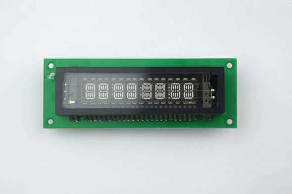

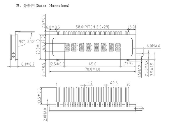
Mon
01
May
2017
FUTABA 271 VFD Module for Arduino /AVR/PIC/STM/ARM/PI 5V ready
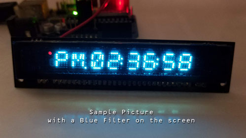
Please use Adobe ACROBAT reader to open the PDF,you will find .INO source code inside the PDF in the attached files part.
Specifications(For reference only):
Panel Name: FUTABA 8-BT-271NK (16-segment style char in dot looking)
Panel Size: 80mm*14mm;
Panel Color: Green(chars)+Red(dot and bluetooth mark);
Supply: 5V DC;
Max Current: ~150 mA;
Module Size: 90mm(L)*20mm(W)*9mm(H)(*17mm(H)with the 2.54mm pins);
PCB Size: 90mm*20mm;
PCB Color: Black/Green;
Weight: ~128g;
The module works with any 5V DC MCU, especially designed for ARDUINO!
Features:
1).5V Ready, easy to be used. Can connect to your ARDUINO UNO board with only 3 singal wires;
2).High efficiency power circuit, no transformer, no heat, Low HV, very safe, High Brightness;
3).All SMT components, very thin PCB, easy to be drivered;
4).All segments in the VFD pannel can be lighted up, including the dots,colons;
5).Contains over-current protection, and reverse connection protection circuits;
6).Open source ARDUINO NUO source code, pure C code, provide high level vfd_printf() function, easy to be used, also provide a simples clock source code which you can adjust the Hour and Minute for ARDUINO UNO.
7).Simple 3-wire SPI interface, with EN pin, support adjusting the global brightness and shutdown the High Voltage and Filament Supply completely.
Interface:
3-wire SPI: DIN/CLK/LATCH(STROB)
+5V/GND/EN - High voltage & filament supply enable(optional)
For video(s):
https://youtu.be/aXa5hoYy47s
Cell phone filmed
For more information:
http://vfdclock.jimdo.com
The source code is for ARDUINO UNO, running in ARDUINO V1.04.


Sun
09
Apr
2017
New-Plug-able IN-12 6-tube NIXIE clock with middle colons

This Plug-able IN-12 6-tube NIXIE clock can be placed horizontally or tilted with tilt-back legs installed.
All NIXIE tubes and the middle neon bulbs(colon) are installed via electronic pins. You can replace the tubes and the middle colons by yourself by hand without using any tools.
Old and Historical instructions:
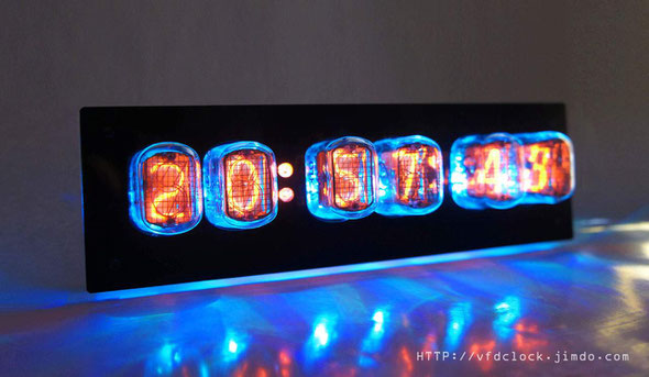
Notice:
In order to drive the NIXIE tube, some internal equipment are under the High Voltage (up to ~180V DC), please do not use this clock outside or in any wet conditions, please do not touch any part inside the clock when power supply is turned on. Always keep it away from kids.
Specifications:
Tube Name: IN-12(Made in the U.S.S.R.)
Clock Supply: 5V DC via USB;
Max Current: ~650mA;
Clock Size: 198mm(L)*61mm(W)*22mm(H)(~43mm(H)with IN-12 tubes installed);
PCB Size: 186mm*50mm;
PCB Color: Black;
Weight: 192g;
Working videos:
https://youtu.be/ngtVQRtzfBo
https://youtu.be/i-l5gwxUlu0
Features(For reference only):
1).5V USB powered, easy to be used. Can connect to your computer's USB plugs directly (*Recommend 5V/1A or up USB power adapter).
2).High efficiency HV circuit, you get almost no heat in 24*7 working condition;
3).All SMT components, very thin PCB; Static driving, No Flashing, High Brightness;
4).Support 12H or 24H display modes. Leading zero blanking is programmable.
5).Display date in all format: YY.MM.DD or DD.MM.YY or MM.DD.YY or even MM.YY.DD; Can display week info too.
6).Support a lot of different Effects: Normal/ Fading/ Cross Fading/Flash /Loop /Random Loop/ Scroll + Mix1/mix2 for displaying time(* Effects may will be changed in the future).
7).High accuracy RTC inside, DTCXO (temperature compensated crystal oscillator) version, High Stability, Highly accurate. It has ±1.9ppm (Equivalent to ±4.94s seconds of month deviation) under 0ºC~+40ºC. Usually you don't need to set the time
for over a year.
8).Simple setting by using 3 buttons only and supports IR remote control (optional). Also has a new SNOOZE button.
9).Three alarms with weekends ON/OFF support can be controlled individually.
10).Three programmable Auto Power ON/OFF mode, can turn ON/OFF NIXIE tubes in any time you want. This function can save tubes life.
11).CR1220 battery socket on-board for the RTC power which keeps RTC running during power outages. (*Prepare the CR1220 battery by yourself.)
13).Tri-colored RGB LED mounted under the each NIXIE tube. These LED(s) can display pre-defined auto
color change effects.
14).Store user settings in non-volatile memory.
15).Beautiful CAD designed acrylic case made using a laser cutter makes the clock look beautiful. You can assemble/disassemble the case by using only
4 screws on the bottom of the case. The case also has 2 tilt-back legs as feet on the bottom of the case to placed the clock tilted for easy to read the time on desktop.
16).Can install Temperature Sensor(optional) ;Can install wireless module(optional) for receiving the outside info, like the wireless
temperature sensor's data and the GPS time sync data, etc.

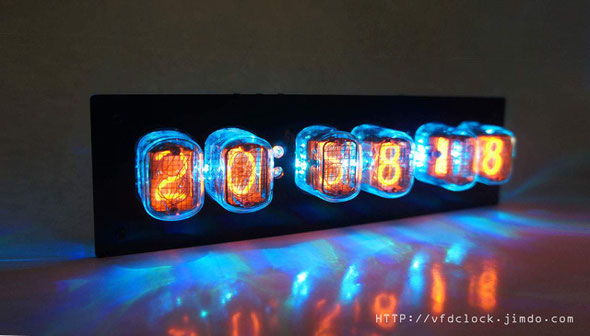
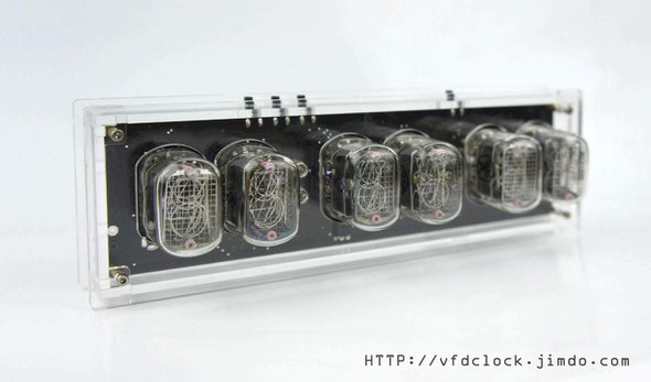


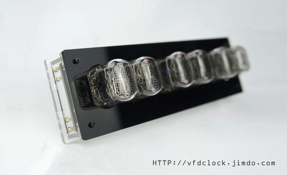
Product Change Notification in the New Version:
Sat
12
Nov
2016
New-[HV12-Pro]-12W-Small Size-12V to 380V(Max) High Efficiency PSU for Audio Application
High efficiency High Voltage 380V (Max) Power Supply Modulefor Audio
Brand New Design,High Frequency,High Power,Hig Efficiency.
Have tested by myself,under 10W output,working in 24*7 condition,the module got almost no heat!
Very small size,only 43mm*24mm, with STD. Pins,can accept 12V~15V input,output is adjustable;
Can output 380V(Max) with loader on at ~10W power with no problem;
Max efficiency up to 89.5%,even under the 380V,25mA ~10W output condition,still have about 85% efficienty.(*May have ~3% error because of the accuracy of the equipments);
Description:
1. This is a newly designed high voltage power converters;Can accept
12~15V DC in,and output ~380V DC(Max),
output is adjustable by using a
ex. resistor;
2. Have increased the frequency up to about 120kHz to get more noiseless output;
3. High quality transformer on-board to low down the noise;
4. It contains an ENABLE pin to turn the convert on/off,and can be controlled by an regular logic signal,like a MCU's GPIO
PIN.
5. Module contains input reverse polarity protection and short protection circuit via current limiting.
6. No audible noise;
7. Standard 0.1"(2.54mm) pins, easy to
be used, can use DuPont-Wires etc.
(* Remember to seperate the dupont-wire when connect
to the 380V part.)
Tips:
1.Please control the input current in <=1A for the low heat working state,if need more power output,you can increase the input voltage;
2.Please use high quality and stable input DC source,make sure the max input voltage is not over the max range;
3.We recommend using 12V as input;If need more output power
can use 15V input.
4.Do not go over power/Heat/voltage/current, will damage the
MOSFET or IC or Transformer on board.
Simple test by myself:
By using 12V input,output 380V drive a 15K Std. Resistor,the results shown below:
Input:12V, 0.95A;
Output Voltage:380V with the 15K load on;
Output Current: 25.3mA;
Power output: 9.62W;
Efficiency: ~84.33%;
No audible noise;
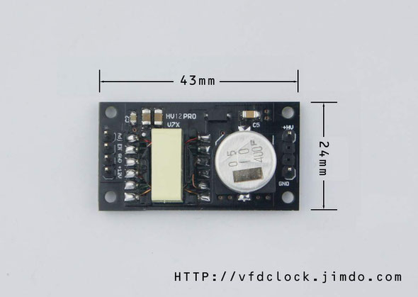

Sat
17
Sep
2016
USB Powered VFD48 Analog-style Unique Round VFD Clock Assembly Instructions
If wanna buy this kit,please check our store:
USB Powered
VFD48 Analog-style Unique Round VFD Clock
Assembly Instructions
Contents
Notice
Building it
Preparing
Step 1: USB Power In and MCU part
Step 2: RTC part
Step 3: Filament Driver part
Step 4: Negative High Voltage part circuit
Step 5: CDS and IR part
Step 6: VFD drive Chip
Step 7: First Testing
Step 8: Cleaning Circuit Board
Step 9: Buzzer part
Step 10: Buttons part
Step 11: Test the buttons, buzzer, and VFD panel
Step 12: Solder the VFD48 Panel
Step 12: Solder the Extras:
Circuit and PCB
Notice
For assembling the VFD48 clock you need to have the skill of soldering SMD components. We use a Hakko FX-888 Soldering Station (with CF2 Iron Head) and a Hot air blower station. We use 183℃(degree C)low melt temperature solder wire S60, 0.5mm(Dia.), Brand Almit.
For how to solder the SMD components, we recommend:
https://www.hakko.com/english/tip_selection/type_bc_c.html
https://www.hakkousa.com/video/
Please do not change any equipments of the KIT or you may not be able to get the clock working.
If already have the skill of soldering the SMD components, it is easy for you to assemble the clock, please check the circuit diagram carefully and follow the steps shown blow.
We do not recommend you to solder the components in random order or if it has problems you will need
more time for de-soldering and debug, we recommend you follow the steps in this instructions that you can do part test after finished each
step.
For more info & update, please visit HTTP://vfdclock.jimdo.com
Or contact us: zjjszhangf[at]gmail.com
Thanks for choosing our product.
Building it
Well, because of the circuit is module based and not very complicated, all you need to do is get all the components in the right position and make sure no short before you plug the power in. We will show the soldering steps blow.
Preparing
1. Please print out the PCB installation diagram by yourself, the Circuit diagram is no need for soldering job, print it or not depends on you(Note: May only have the paper circuit diagram in the KIT with no digital version provide.);
2. Check all the components in the kit bag, make sure nothing is missing (You can do this on a A4 white copy paper);
3. We recommend using a soldering station and small soldering tip for soldering this kit (we use F2 or CF2 type tip). If you have a hot air gun(or Hot air blower station) tool for soldering, that will be great. We recommend using ~180℃ type soldering tin for this job. Please do not use the high temperature soldering tin in this project, you may damage a lot of SMD components or the PCB;
Step 1: USB Power In and MCU part
Solder the [USB Power In] part first; This part contains a USB socket and a 1206 size RESETTABLE fuse.
For soldering the USB socket, we recommend solder the 5 middle Pins first, then flip the PCB to the other side and use long flat nose pliers to band the two fixed legs of the USB socket a little bit close then solder these two fixed legs.
Then solder the 1206 FUSE, usually in golden color with mark [4] on it, easy to find.
After soldering these two components, you can plug the USB power in and measure the fuse output pad to see if it has 5V output.
The next part of this step is soldering the main MCU chip, it is a LQFP32 package MCU with [105K6T6](or 005K6T6) mark on it. Please check the first legs position. For soldering the QFP stuff like this, we recommend that you use a short Polyimide Tape to glue the chip on the correct location of the PCB first, then solder one corner, if all fine, solder the other side pins in the next, then the rest sides' pins.
After finish soldering the MCU chip, double check all the pins, make sure no short. Then solder two capacitors blow the MCU chip(1uF and 0u1F), the 1uF one is the key component, must be installed or the MCU won't work.
Step 2: RTC part
In this step, you need to solder the RTC (Real Time Clock) part components, it contains 3 components, the major one is the RX8025 RTC all in one chip in SOP14 package, it may have the mark RX8025AC or RX8025T mark on the surface depends on the kit's version. Please solder the chip in the correct direction, please control the iron's temperature, and solder it fast, and take care of the ESD(Electro Static Discharge) control.
Then solder the diodes D1 in sot-23 package with [5C6] mark and the 0u1F capacitor.
(*Please note that RX8025AC and RX8025T are not the compatible chips, if damaged the chip ,please use the same mark chip to replace).
You can try to plug the 5V USB power, if the RTC chip and the MCU in working, you can find the 1Hz(or 2Hz) signal in the 1Hz testing pad(you can use oscillograph if you have).
If you want, you can install the CR1220 Battery Socket too at this step, recommend to cut the left&right pads of the socket a little bit short for easy to solder.(Note: The straight metal pad part in the socket is the [+] pad, do not go invert;
Step 3: Filament Driver part
Now we can solder the filament driver part components. This part of the circuit contains a H bridge which created by 4 MOSFETs and other components for EK level shift with the -HV part circuit.
This part of the MOSFETs components are SOTt23-3 MOSFET(A1SHB & A2SHB mark) and resistors and capacitors, please do not change the C3+C4(1uF/50V) capacitors value(only use the caps in the kit).
And it also contains a 6V5 Z-diode inside, usually in glass package with a round color bar(usually in blue or black) at the cathode side, easy to find, please solder it in the right direction.
After this step, you can plug the 5V USB power in ,then plug the VFD48 panel in (Please do not solder the panel at this time), press the panel a little bit to make sure the pins touch the PCB pad well, when under the black environment, you can see the filament inside the panel will be light up in a little bit dark red color. Or you can measure the filament pins with oscillograph, you can see the AC output.
Step 4: Negative High Voltage part circuit
The Negative High Voltage part circuit is made by the -HV boost DC-DC chip, it is in SOT23-5 package with LTKF/LTES/LTRA mark on surface; Just follow the PCB diagram to solder this part of the circuit components. Want to notice that please control the soldering temperature and make sure the 10Uh inductor pad is be soldered correctly.
And for testing this part of the circuit, you can measure it's output via two side of the C11 capacitor or the [-HV] testing pad on the PCB, if installed correctly, it will have >=25V(or -25V) HV output.

Step 5: CDS and IR part
The CDS and the IR part (optional) will be easy; We recommend you to solder the CDS part first with two 22K resistors and one CDS sensor(CDS should be installed on the PANEL side), and the 0u1F capacitor for the IR sensor; We can solder the IR receiver later (if it has the IR function).

Step 6: VFD drive Chip
Flip the PCB to the other side then we can solder the components on this side. The major chip on this side is PT6315 VFD Chip in LQFP-44 package; Use the same skill of soldering the MCU to solder this chip. Also please double check the chips' pins carefully after soldering.(* Please note that the PT6315 chip may have two round hole marks on its surface, the small hole marks the first leg.)
Please solder the 3PCS 0u1F capacitors and 100K resistor (* key component, do not change the value) too.
Step 7: First Testing
After finished all the 6 steps shown up, now we can plug the VFD48 panel in the PCB(Do not solder it!) and plug the USB power in, use hand to push the panel a little bit up to make sure all the legs touched the pad; If all fine the clock will started displaying and ticking, please check all the segments inside the panel to see if can be light up correctly. If some segments do not light up, please check if some legs of the panel did not contact the pad correctly or tightly or some legs of the PT6315 chip did not be soldered correctly. If the two or more segments are lighted up together, may have the short among the PT6315 legs.
If all fine, unplug the panel we can do the next step.
Step 8: Cleaning Circuit Board
You can use the household rubbing alcohol and a toothbrush to remove the solder flux on the PCB. If available, the anhydrous alcohol (used for electronics cleaning) works much faster. Blot the cleaned area with a non-linting tissue (like Kimwipes EX-L) or a clean towel or you can do it in your own way.
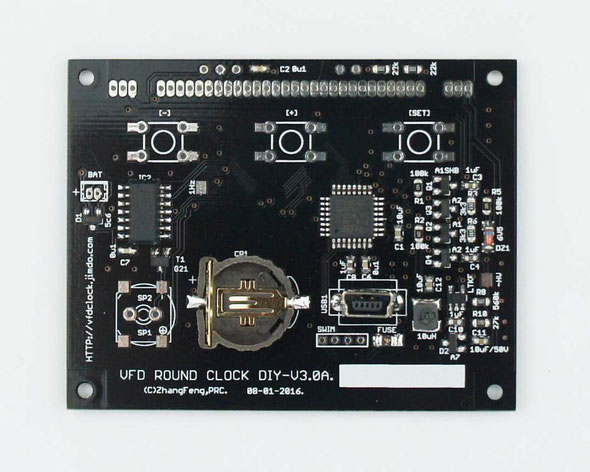

Step 9: Buzzer part
Buzzer Part is easy, first solder the [G21] Digital Transistor (Note: If damaged this component, you can replace it with the SI2302[A2SHB] N-MOSFET);Then Solder the buzzer part, we have two types of the buzzer, one is the SMD Version, the other is the DIP version, please solder the one which you find in the KIT.
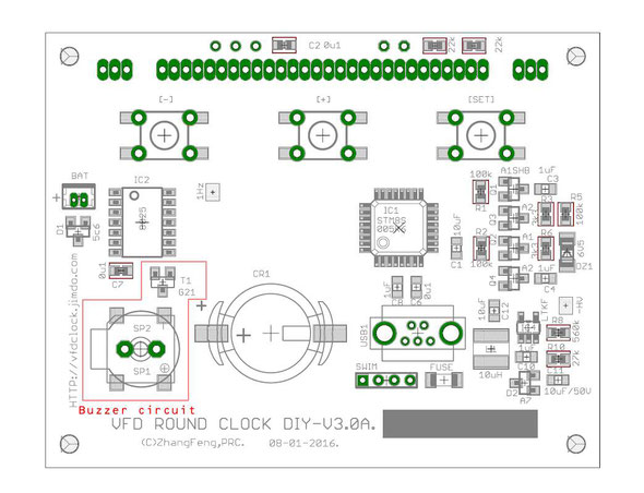
Step 10: Buttons part
There are 3PCS of the buttons on the PCB, usually you will find 3PCS 6*6 SMD version of the buttons in the KIT. If you have enough soldering skills, you can solder those buttons directly or we recommend that you use long flat nose pliers to band the button legs straight, then you can plug the buttons inside the PCB holes, and then solder the legs.
Step 11: Test the buttons, buzzer, and VFD panel
After finished all the steps shown up, we have almost finished assembling the PCB. At this time, we recommend plug the USB power in, then click the button(s) to see if all the button(s) in working, and to see if the buzzer can beep when you click the button.
If all fine, you can unplug the USB power, then plug the VFD48 PANEL in the PCB holes, then plug the USB power back to give it a light up test.
We suggest that you use your hand to push the vfd48 panel a little bit up to make sure all the VFD panel legs touch the PCB holes, if all fine, the VFD48 panel can be light up and will start to display the time, please wait for at least one minute to check all the segments inside the panel to make sure all can be light up properly.
Step 12: Solder the VFD48 Panel
When soldering the VFD48 panel, we used to solder the left and right two legs first, then adjust the high of the legs(by using the solder) to make sure the panel has the same height at the both sides. Then you can use sharp scissors to cut all the legs short and solder all the legs (Because of the legs are really close, please be patient and do it carefully).
After finished assembling the PCB, you can do the test again.
Then you can clean the buzzer and the buttons and panel legs by using the cotton swab with alcohol (or other things you have).
Notice:
Please do now wash the Buzzer/Buttons by alcohol or will be damaged!
Please do not wash the VFD48 Panel in the ultrasonic wave cleaner, may damaged the filament!
If necessary, you can add a small size (like 0.5cm*1.5cm) 3M double stick foam tape to glue the panel on the PCB.
Step 12: Solder the Extras:
If have IR function, you need to solder a IR receiver on the front side. We recommend you band the IR receiver legs in 90 degrees (aware the direction), then plug it inside the PCB holes then solder it. Because of the IR receiver is heat sensitive equipment, please control the temperature and solder it fast.
Wed
31
Aug
2016
New-USB powered-IN-18 6-tube NIXIE clock with glass tube middle dots
This is the newest design USB powered IN-18 6-tube clock with glass tube middle dots,all plug-able design.
All the NIXIE tubes and the middle dots can be replaced by hand directly via the electroic socket pins.
Highlights:
Usb Powered,high efficiency power module,up to 90%,when under 5V,all 6 tubes in the highest brightness and with all LEDs on,the current is about <=1A only!!!
8-level global brightness with no blue dot.

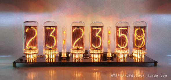
Sat
20
Aug
2016
New-Plug-able IN-14 6-tube NIXIE clock with glass tube middle dots and with AC driving circuit
This is the newest design with glass tube middle dots drived by AC circuit.
All the NIXIE tubes and the middle dots can be replaced by hand directly via the special designed sockets.
Highlights:
We have updated the middle dots to [2pcs ~4mm neon bulbs with glass tube outside], the middle dots can be installed via the socket [Pluggable],thus you can
replace it by hand too.And Yes,NEW AC driver circuit for the middle dots,thus 2 segments
inside the neon bulbs all can be light up together!!!
This is the Pluggable version, NIXIE tubes can be installed via "SPECIAL THROUGH-HOLE FEMALE SOCKET PINS",you can replace the IN-14 NIXIE
tubes by yourself by hand.
国内用户自行请连接以下地址观看工作视频:
http://v.youku.com/v_show/id_XMTY5NTA4NDYzMg==.html
http://v.youku.com/v_show/id_XMTY5NTA4ODc5Ng==.html
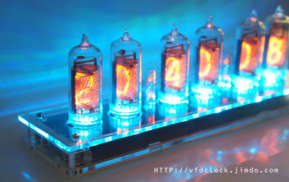
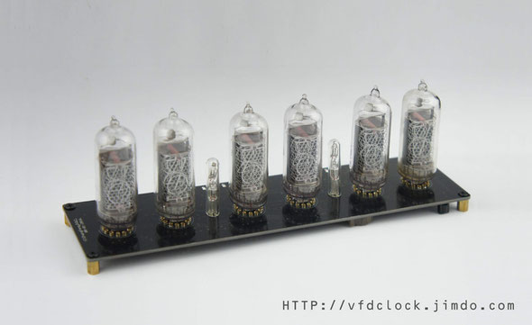
Product Change Notification in the New Version:
1.Add the Li-Battery drive-able function(Optional),thus it can work with the Li-poly battery only without the USB power if has this function
installed;
2.Update the software,now can show the AM/PM in [.12Hour mode] by using the one dot inside the tube;
3.Have 2 Slot Machine Effcts,and you can turn on/off the Slot Machine by
setting;
USB Powered;Slim design;Module based structure;Low heat;Static driving;No Flashing;
Specifications(For reference only):
Tube Name:IN-14(Made in the U.S.S.R.);
Tube Diameter:18mm;
Tube Height:55mm(approx including glass nipple);
Digit Height:17mm;
Digit Width:10mm;
Clock Supply: 5V DC via USB;
Max Current: ~550mA(~900mA when in charging mode if has the Li function);
PCB Size:186mm*45mm;
PCB Color: Black;
Features(For reference only):
1).5V USB powered, easy to be used. Can connect to your computer's USB plugs directly (* In some computers you may
need to use the USB Cable that Have Two USB Connectors at the End.).
2).High efficiency HV circuit, you got almost no heat in 24*7 working condition;
3).All SMT components, very thin PCB, only 8mm(Max) high with the Top & Bottom components; Static driving, No Flashing, High Brightness
4.Support 12H or 24H display modes. Leading zero blanking is programmable.
5.Display date in all format: YY.MM.DD or DD.MM.YY or MM.DD.YY or even MM.YY.DD; Can display week info too.
6.Support 8 different Effects: Normal/ Fading/ Cross Fading/Flash /Loop /Random Loop/Scroll/Mix1/Mix2 for displaying time. All tubes' 0~9 segments tube can be lighted up;
7).High accuracy RTC inside,±1.9ppm, usually ±4.94 seconds per month.
8).Simple setting by using 3 buttons only.
9).Three alarms with weekends ON/OFF support can be controlled individually.
10).Three programmable Auto Power ON/OFF mode, can turn ON/OFF NIXIE tubes in any time you want. This function can save tubes life.
11).Support [SNOOZE] key.
12).Cr1220 RTC battery socket on board keeps RTC running during power outages.
13).Tri-colored RGB LED mounted under the each NIXIE tube. These LEDs can display different colors at the same time, with a lot of pre-defined auto color change effects.
14).Store user settings in non-volatile memory.

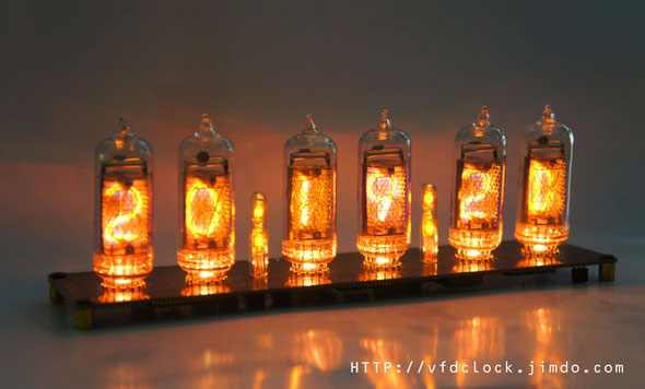
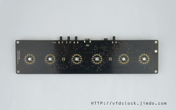
Tue
26
Jul
2016
Plug-able USB Powered-Li-poly battery drive-able ,Two-Digit IN-18 NIXIE Tube Clock-Pro.
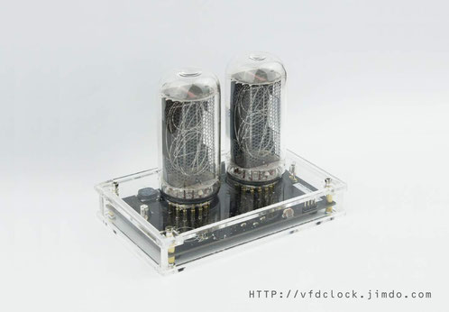
Plug-able USB Powered-Li-poly battery drive-able
Two-Digit IN-18 NIXIE Tube Clock Pro.
New design, by using two In-18 NIXIE tube to display the Time/Date/Temperature
*Improved the HV circuit,small size,high Efficiency.You get almost no heat under 24*7 working condition;
*Improved the RTC rechargeable battery,now can last over weeks when fully charged;
*Improved the software,add self power on testing function,add [FLASH] switching effect;
*Can install Li-poly battery charging circuit(optional), thus you can light the clock up by using the Li battery;
Specifications:
Tube Name: IN-18 (Made in the U.S.S.R.);
Tube Size: 30mm(dia);
Tube Height: 68mm(no including the legs and the glass nipple);
Digit Height: 40mm;
Digit Width: 22mm;
Clock Supply: 5V DC via MINI-USB;
Working Current: ~450mA;(~850mA in Li-poly battery charging mode);
Clock Size: 104mm(L)*66mm(W)*20mm(H)
PCB Size:94mm*56mm;
PCB Color: Black;
Weight:75g(weight no tube installed);
The clock works with any standard USB power supply,use only high-quality adapter!
The clock works with any standard USB supply, use high-quality adapter only!
Features:
1).5V USB powered, easy to be used. Can connect to your computer's USB plugs directly;
2).High efficiency HV circuit, you get almost no heat in 24*7 working condition;
3).All SMT components, very thin PCB, Bottom component has only 6mm(max) high; Static driving, No Blue Dot, No Flashing, High Brightness;
4).Support 12H or 24H display modes, can show "." as "A/P" in 012H time format. Leading zero blanking is programmable;
5).Display date in all format: YY.MM.DD or DD.MM.YY or MM.DD.YY or even MM.YY.DD; Can display week info too;
6).Support 5 different Effects: Normal/ Fading/ Cross Fading/Slow Fading /Loop/Flash for displaying time. All the segments in the IN-14 tube can be lighted up, include the Left & right
dots;
7).High accuracy RTC inside, factory calibrated to ± 5ppm, ±13 seconds (Max) per month;
8).Simple setting by using 2 buttons only and supports IR remote control (optional) ;
9).Three alarms with weekends ON/OFF support can be controlled individually;
10).Three programmable Auto Power ON/OFF mode, can turn ON/OFF NIXIE tubes in any time you want. This function can save tubes life;
11).8-level adjustable NIXIE tube bright with Auto-brightness feature (it is able to adjust the tube brightness depending on the current environment);
12).Rechargeable Backup Battery or Farad capacitor keeps RTC running during power outages;
13).Tri-colored RGB LED mounted under the each NIXIE tube. These LEDs can display different colors with a lot of pre-defined auto color change effects.
14).Store user settings in non-volatile memory;
15).CAD designed acrylic case made using a laser cutter makes the clock look beautiful. You can assemble/disassemble the case by using only 4 screws on the bottom of the case. The case also has 4
bumpers as feet on the bottom of the case in order to stop to prevent case's damage;
16).Can install Temperature Sensor(optional) ;Can install Li-poly battery charging circuit(optional),thus you can light
the clock up with Li-poly battery only;
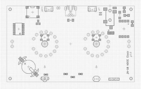
under construction...

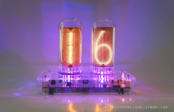
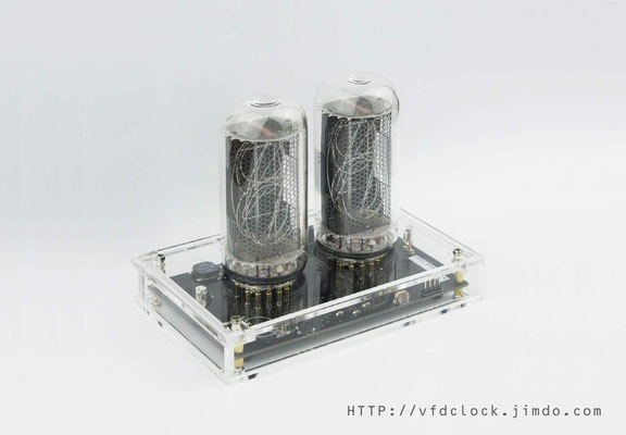


Wed
08
Jun
2016
KIT-DIP-NIXIE Power Supply Module-10W-MC34063 High Voltage

Build a High Voltage power supply
by using the MC34063 Chip
DIP Version
This kit allows you to make an MC34063 based boost PSU, which can accept a 12V DC input and output ~210V DC for powering NIXIE tubes and others that require high voltage. It is a very common circuit, the key point is the selection of the Inductor and the Mosfet.
Please do not change any equipment of the circuit or you may not be able to get the target HV output or the module may work under the lower efficiency state.
For more info & update, please visit HTTP://vfdclock.jimdo.com
Or contact us: zjjszhangf@gmail.com

How it works
The circuit is very simple, we use one of the most common switching regulators on the planet-the MC34063 chip. The circuit is the based on the Step-up structure. MC34063 contains a NPN output only structure, in order to drive the Mosfet, we add a 1K pull-down resistor(R2) to get the low side signal. And because we need to convert the 12V DC input to the ~210V DC output in one step, the ration requirement is very high, so we add a speed up circuit by using a PNP transistor(Q2) and a schottky diode(D2) to speed up the drop side of the driving wave. Other part of the circuit is very simple, please check the MC34063 official PDF file by yourself.
Building it
Well, because of the circuit is pretty simple, all you need to do is get all the component in the right position and make sure no short before you plug the power. And the kit contains NO SMD component, no need to have the skills of soldering the SMD stuffs. We show no the soldering steps, just remind the matters needing attention blow.
1. Please print out the PCB installation diagram by yourself, the Circuit diagram is no need for soldering job, print it or not depends on you;
2. Check all the component in the kit bag, make sure nothing is missing (You can do it on a A4 white copy paper);
3. We recommend using a soldering station and small soldering tip for soldering this kit(we use F2 or CF2 type tip). we
recommend using ~180℃ soldering tin for this job. Please do not use the high temperature soldering tin in this project, you may damage the PCB or
component;
4. The PCB has 2-side, so solder on which side depend on your choice and also depends on the component;
Tips:
1. Take care of the C1 and C2(Aluminum Electrolytic Capacitor), it has polarity, do not install it in invert direction;
2. The main HV mosfet (Q1), if the mosfet in the kit is the TO220 package, you just need to plug it in the place, then cut the legs short and solder it, if the package is the TO263 package, band left&right legs straight by using needle-nose pliers or other tools; The mosfet's mark surface must be face the frond side of the PCB(face the MC34063 chip side).Double check the mosfet part after soldering, make sure it contains no short, it is very important!
3. Recommend do not wash the trimmer or may damaged the trimmer, also do not wash the Inductor or may cause the sound when MC34063 works under ON/OFF mode. If the inductor has been washed, recommend to re-coat it with the Plasticote (We use CRC-70);

The smoke test
Put the circuit board on an insulating surface, connect no loader to the output side, connect the input pin to a 9~12V DC source. If you have a current limited supply that will be perfect. Or you can try to use a 9V small home using MN1604 (6LF22) battery to prevent to burn something at the first time.
If all fine, the max output usually can go up to ~210V with no problem.
The whole circuit is pretty easy, no need to adjust.
Identifying the parts of your power supply kit
The following guide should help you to identify the parts and assemble it successfully
Resistors
All the resistors contains color mark on it's surface. The 0R1 is the biggest one ,and the 1M is the big one, easy to identify. Others may have the same size, if can't read via the color rings, measure it.
Diode
The diodes will be marked with HER105/SF-16/SF-18(black one), 1N5819(black one), and 1N4148(the small glass one), the cathode side contains a black or white mark.
Capacitors
Kit contains 4 small capacitors, All with the number on its' surface.
And for the Aluminum Electrolytic Capacitor, usually the longer lead is positive, or if both leads are the same, the negative is clearly marked with a big line or minus symbol running down the side of the case.
The MOSFET
The MOSFET will be marked 27N25/45N25 or other numbers, please note the mosfet marks surface must be installed face to the MC34063 chip side.
The MC34063 chip
MC34063 chip in this kit is DIP8 package, make sure it is installed the correct way around, just follow the chip direction shown on the PCB.
Partlist
Assembly variant:
|
Qty |
Value |
Device |
Parts |
Mark |
|
Resistors |
||||
|
1 |
R100=0R1 |
R-EU_0411/12 |
R1 |
The Biggest One |
|
1 |
1M 1/4W 250V |
R-EU_0207/10 |
R4 |
The Big One |
|
1 |
1k0 |
R-EU_0204/6 |
R2 |
|
|
1 |
33k |
R-EU_0204/5 |
R3 |
|
|
1 |
5k6 |
R-EU_0204/6 |
R6 |
|
|
Capacitors |
||||
|
1 |
0u1F(100nF) |
C-EU025-024X044 |
C3 |
104 |
|
1 |
390pf |
C-EU025-024X044 |
C4 |
391 |
|
1 |
68pf |
C-EU025-024X044 |
C5 |
68 |
|
1 |
300pF |
C-EU025-024X044 |
C6 |
301 |
|
Diode and Trans |
||||
|
1 |
PNP 8550 |
TRANSISTOR_PNPTO92 |
Q2 |
8550 |
|
1 |
HER105/SF-16/SF-18 |
DIODE-DO41-6.5 |
D1 |
HER105|SF16|SF18 |
|
1 |
IN4148 |
DIODE-DO41-7.6 |
D2 |
Glass diode |
|
1 |
1N5819 |
DIODE-DO41-7.6 |
D3 |
1N5819 |
|
Mosfet/IC/Others |
||||
|
1 |
100uH |
INDUCTANCE_US11X11PLUG |
L1 |
|
|
1 |
330uF/35V |
CPOL-EUE5-10.5 |
C1 |
220~470uF |
|
1 |
10uF/250V |
CPOL-EUE5-10.5 |
C2 |
10~15uF |
|
1 |
MC34063-DIL |
MC34063-DIL |
IC1 |
MC34063 |
|
1 |
MOSFET-n |
MOSFET-NCHANNELTO220V-BH |
Q1 |
TO220/TO263 |
|
1 |
20k |
R-TRIMM3296W |
R5 |
Blue Trimmer |
|
PINS |
||||
|
2 |
|
M02PTH |
HV, VIN |
|
exported from MC34063HV-05D-KIT
The defferences between 210V and 180V is the MC34063 chips and the C4+C5 capacitor which define the freq of the circuit.
For the 210V MAX version,we use the ON MC34063 with the 390pF+68pF Caps;
For the 180V MAX version,we use the other MC34063 with the 560pF Cap;
Sun
24
Apr
2016
Plug-able USB Powered-Li-poly battery drive-able ,Two-Digit IN-14 NIXIE Tube Clock-Pro.
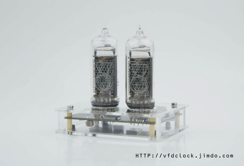
Plug-able USB Powered-Li-poly battery drive-able
Two-Digit IN-14 NIXIE Tube Clock Pro.
New design, by using two In-14 NIXIE tube to display the Time/Date/Temperature
*Improved the HV circuit,small size,high Efficiency.You get almost no heat under 24*7 working condition;
*Improved the RTC rechargeable battery,now can last over weeks when fully charged;
*very thin PCB,the MAX height equipment under the PCB is the 6mm*6mm button;
*Improved the software,add self power on testing function,add [FLASH] switching effect;
*Can install Li-poly battery charging circuit(optional), thus you can light the clock up by using the Li battery;
Specifications:
Tube Name: IN-14(Made in the U.S.S.R.)
Tube Diameter: 18mm;
Tube Height: 55mm (approx including glass nipple);
Digit Height: 17mm;
Digit Width: 10mm;
Clock Supply: 5V DC via USB;
Max Current: ~200mA(~500mA in Li-poly battery charging mode);
Clock Size: 68mm(L)*50mm(W)*70mm(H)(with IN-14 tube installed);
PCB Size: 58mm*41mm;
PCB Color: Black;
Weight: ~60g;
The clock works with any standard USB supply, use high-quality adapter only!
Features:
1).5V USB powered, easy to be used. Can connect to your computer's USB plugs directly;
2).High efficiency HV circuit, you get almost no heat in 24*7 working condition;
3).All SMT components, very thin PCB, Bottom component has only 6mm(max)
high; Static driving, No Blue Dot, No Flashing, High Brightness;
4).Support 12H or 24H display modes, can show "." as "A/P" in 012H time format. Leading zero blanking is programmable;
5).Display date in all format: YY.MM.DD or DD.MM.YY or MM.DD.YY or even MM.YY.DD; Can display week info too;
6).Support 5 different Effects: Normal/ Fading/ Cross Fading/Slow Fading /Loop/Flash for displaying time.
All the segments in the IN-14 tube can be lighted up, include the Left & right dots;
7).High accuracy RTC inside, factory calibrated to ± 5ppm, ±13 seconds (Max) per month;
8).Simple setting by using 2 buttons only and supports IR remote control (optional) ;
9).Three alarms with weekends ON/OFF support can be controlled individually;
10).Three programmable Auto Power ON/OFF mode, can turn ON/OFF NIXIE tubes in any time you want. This function can save tubes life;
11).8-level adjustable NIXIE tube bright with Auto-brightness feature (it is able to adjust the tube
brightness depending on the current environment);
12).Rechargeable Backup Battery or Farad capacitor keeps RTC running during power outages;
13).Tri-colored RGB LED mounted under the each NIXIE tube. These LEDs can display different colors with a lot of pre-defined auto color change
effects.
14).Store user settings in non-volatile memory;
15).CAD designed acrylic case made using a laser cutter makes the clock look beautiful. You can assemble/disassemble the case by using only 4 screws
on the bottom of the case. The case also has 4 bumpers as feet on the bottom of the case in order to stop to prevent case's damage;
16).Can install Temperature Sensor(optional) ;Can install Li-poly battery charging circuit(optional),thus you can light the clock up with
Li-poly battery only;


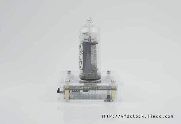
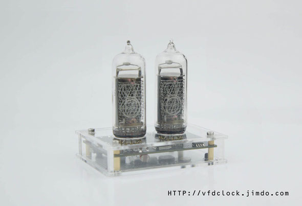
Thu
14
Jan
2016
KIT-Create the Middle Dot Comma for IN-18 NIXIE clock
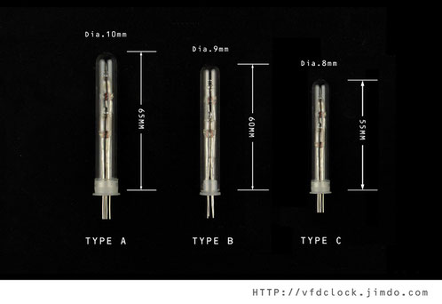
Currently we have more types of the difference size of the glass tube,you can select the size which fits your clock.
Tube Size:
[TYPE A]: Glass part Size: 10mm(Dia.)*~65mm(Height)-(~8mm(Dia.) inner); The plastic plug is plugged
outside the tube;
[TYPE B]: Glass part Size: 9mm(Dia.)*~60mm(Height)-(~7mm(Dia.) inner); The plastic plug is plugged inside the tube;[TYPE C]: Glass part Size: 8mm(Dia.)*~55mm(Height)-(~6mm(Dia.) inner); The plastic plug is
plugged outside the tube;
With plastic plug under the bottom of the tube;
How to make it by yourself:
![This is [TYPE C] dia.8mm*55mm(H)](https://image.jimcdn.com/app/cms/image/transf/dimension=590x10000:format=jpg/path/sb03fefd490221d21/image/i7d0122d9675ac98e/version/1452865523/this-is-type-c-dia-8mm-55mm-h.jpg)
Here is the stuffs you need:Glass tube,Plastic plug,NE-2 neon indicator lamps,Clear heat shrink tubing,2 LEDs (need its' hard legs).
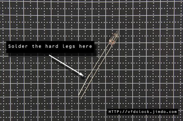
Cut the led legs off,then solder it on the bottom of the neon lamps.In this case,keep the first neon lamp's leg no cut.

Cut the the other neon lamp's leg a little bit short,then solder the led legs on it.

Plug the clear heat shrink tubing on each legs,then heat to shrink it. keep the shrink tubing long enough to cover the soldering part of the connections,but no need to cover all of the legs.

Prepare the plastic plug,mark the drill points out on the surface,recommend 2.54mm (0.1") gap, or you can make your own decision.
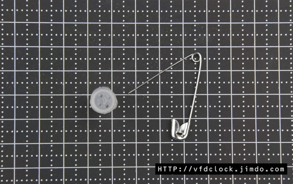
Drill 4 small holes with the tools you have,it's easy,small holes will be fine,no need to drill the big holes.

Plug the Neon lamps inside it.

Plug the neon lamps leg in a big foam, and adjust the location of the lamps.

If you feel necessary,you can fill the epoxy or other stuffs in the plastic plug,adjust the lamps again to make sure it fits your request,then plug the glass tube on it.We use the 3M 5 minutes epoxy which works fine. It's an optional step,if you wanna solder it directly on the PCB,we recommend you fill the epoxy.

Plug the glass tube in the plastic plug,the job is almost being finished.

If you find that the plastic plug is too long, you can use a knife to cut it short,just press the blade down the location you wanna cut,then rotate the whole tube. If the plastic plug has skirt on the bottom side,just put the skirt part outside the edge of the table,then do the same round cut.

After been cured, you can remove the no need part off the glass tube.
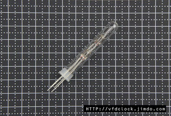
Here is the result.
You can use our through hold female socket pins to install it on the PCB,just cut the outside legs bottom sharp,and leave ~1cm length legs.it will stander there like a tree,and if you did not glue it,you can adjust the location of the lamps and replace the glass tube in the future.
TIP:
For the outside plastic plug ,after you glued with the epoxy,and till the epoxy be solide,if you wanna remove the plastic plug you can cut if off easily with the knife,or you can place a little bit of the vaseline on the inner side of the plug then add the epoxy,can be easily to remove the plug later.

You can use different color of the epoxy like transparent or black,and you can paint the glass tube into red if you need.
Wed
13
Jan
2016
New IN-14 6-tube clock with GPS sync function Standard V2.0
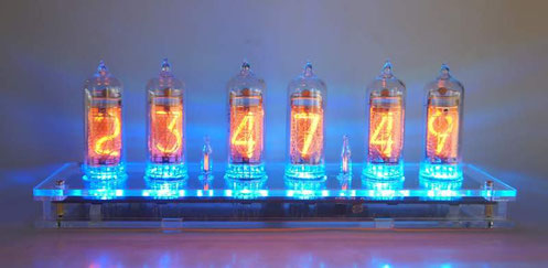
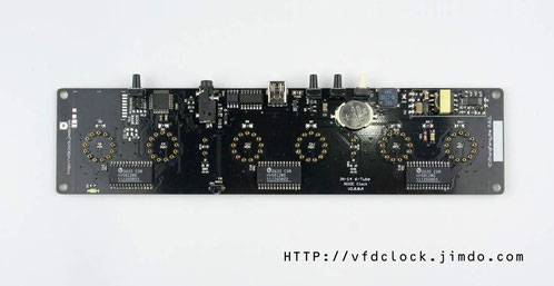

Product Change Notification in the New Version:
1.Add the GPS time sync function via 3.5mm plug;(GPS receiver is no
included!!)
2.By using 3pcs HV5812 chips instead of the transistors for the static driving;
3.Optimized the clock functions,removed the global brightness,CDS function and the dot eff,merged one fade eff,add [SNOOZE] key; Installed a
CR1220 battery socket instead of old RTC battery solution,cr1220 battery is easy to get in the worldwild,etc.
Notice:
In order to drive the NIXIE tube, some internal equipment are under the High Voltage (up to ~180V DC), please do not use this clock outside or in any wet conditions, please do not touch any part inside the clock when power supply is turned on. Always keep it away from kids.
Specifications:
Tube Name: IN-14(Made in the U.S.S.R.)
Tube Diameter: 18mm;
Tube Height: 55mm (approx including glass nipple);
Digit Height: 17mm;
Digit Width: 10mm;
Clock Supply: 5V DC via USB;
Max Current: ~650mA;
Clock Size: 198mm(L)*56mm(W)*17mm(H)(~68mm(H)with IN-14 tubes installed);
PCB Size: 186mm*45mm;
PCB Color: Black;
Weight: 198g;
The clock works with any standard USB supply, please use high-quality adapter or the clock may not work!
Features:
1).5V USB powered, easy to be used. Can connect to your computer's USB plugs directly (* For some old computers you may need to use the USB Cable that Have Two USB Connectors at the end.).
2).High efficiency HV circuit, you get almost no heat in 24*7 working condition;
3).All SMT components, very thin PCB, only 8mm(max) high with the Top &
Bottom components; Static driving, No Flashing, High Brightness;
4).Support 12H or 24H display modes. Leading zero blanking is programmable.
5).Display date in all format: YY.MM.DD or DD.MM.YY or MM.DD.YY or even MM.YY.DD; Can display week info too.
6).Support a lot of different Effects: Normal/ Fading/ Cross Fading/Flash /Loop /Random Loop/ Scroll + Mix1/mix2 for displaying time(* Effects may will be changed in the future).
7).High accuracy RTC inside, DTCXO (temperature compensated crystal oscillator) version, High Stability, Highly accurate. It has ±1.9ppm (Equivalent to ±4.94s seconds of month deviation) under 0ºC~+40ºC. Usually you don't need to set the time
for over a year.
8).Simple setting by using 3 buttons only and supports IR remote control (optional). Also has a new SNOOZE button.
9).Three alarms with weekends ON/OFF support can be controlled individually.
10).Three programmable Auto Power ON/OFF mode, can turn ON/OFF NIXIE tubes in any time you want. This function can save tubes life.
11).CR1220 battery socket on-board for the RTC power which keeps RTC running during power outages. (*Prepare the CR1220 battery by yourself.)
13).Tri-colored RGB LED mounted under the each NIXIE tube. These LED(s) can display pre-defined auto
color change effects.
14).Store user settings in non-volatile memory.
15).Beautiful CAD designed acrylic case made using a laser cutter makes the clock look beautiful. You can assemble/disassemble the case by using only
4 screws on the bottom of the case. The case also has 4 bumpers as feet on the bottom of the case in order to stop to prevent case's damage.
16).Can install Temperature Sensor(optional) ;Can install wireless module(optional) for receiving the outside info, like the wireless
temperature sensor's data and the GPS time sync data, etc.
Mon
02
Nov
2015
Z586M Huge Single Digit NIXIE Tube Clock-Pluggable-USB Powered
Our newly deisgned single digit clock with Ultra Rare Huge Z568M Nixie tube.
Specifications:
Tube Name: Z568M ;
Tube Size:50mm(dia);
Tube Height:107mm;
Digit Height:50mm;
Clock Supply: 5V DC via USB;
Working Current: ~360mA;
Clock Size:90mm(L)*80mm(W)*18mm(H)-(*no including the tube);
PCB Size:80mm*70mm;
PCB Color: Black;
Weight: g(weight with the tube installed);
The clock works with any standard USB power supply,use only high-quality adapter!
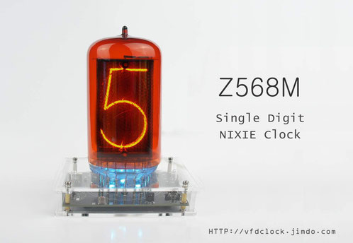

Sample picture from user:eb30177 shows the clock works with Dalibor Farny Nixie tube up and running perfectly !!
Features:
You can replace the tube by yourself without using any tools.
1). 5V USB powered,easy to be used. Can connect to your computer's USB plugs directly.
2). Support 12H or 24H display modes, can show "."as“A/P" in 12H time format.Leading zero blanking is programmable.
3). Display date in all format: YY.MM.DD or DD.MM.YY or MM.DD.YY or even MM.YY.DD.
4). Support different Effs:Normal/Fading/Cross Fading/Slow Fading/Loop for displaying time.
5). High accuracy DTCXO (temperature compensated crystal oscillator) inside,+-4.94 seconds(MAX) per month.
6). Simple setting by using 2 buttons only and supports IR remote control(optional).
7). Three alarms with weekends ON/OFF support,can be controlled individually.
8). Three programmable Auto Power ON/OFF mode,can turn ON/OFF NIXIE tubes in any time you want.This function can save tubes life.
9). 8-level adjustable NIXIE tube bright with Auto-brightness feature(its ability to adjust the tube brightness depending on the current environment).
10). Rechargeable Backup Battery or Farad capacitor keeps RTC running during power outages.
11). Tri-colored RGB LED mounted under the NIXIE tube. These LEDs can display any color with a lot of predefined auto color change effects.
12). Store user settings in non-volatile memory.
13). Beautiful CAD designed acrylic case made using a laser cutter makes the clock look beautiful. You can assemble/disassemble the case by using only 4 screws on the bottom of the case.The case
also has 4 bumpers as feet on the bottom of the case in order to stop to prevent case's damage.
14). Support temperature sensor(optional).
Fri
23
Oct
2015
433M Wireless GPS Time Station for NIXIE clocks (OLED Version)-V1.0
Our 433M Wireless GPS Time Station(OLED version) has passed the two months test,will be online soon.
It receives the GPS signal from the GPS receiver or other sources,and send the time signal via 433M wireless module to the NIXIE clocks.
It contains PA module inside,it can cover 800m range in a open space.
Notice
The GPS antenna (receiver) will need to face upwards with a clear view of the sky to get a good signal. (If the GPS antenna faces with a full view of the sky, it will be perfect.)
Waterproofing is needed when you install the GPS antenna (receiver) outside constantly. Like using a plastic bottle cut in
half or using plastic bag, etc., figure it out yourself.
Please remember to install the 433M wireless antenna before using.
Specifications
Supply: 5V DC via USB;
Working Current: <=250mA;
Size: 70mm(L)*56mm(W)*18mm(H)
PCB Size: 64mm*50mm;
PCB Color: Black;
Weight: ~64g;
Wireless Cover Range: 800m (*In a open space. The range also depends on the antenna, obstructions, interference, and the ability of receiver devices.)
GPS TTL speed: 4800bps.
The item works with any standard USB supply, use high-quality adapter!
Features
1).5V Mini-USB powered, easy to be used. Can connect to your computer's USB plugs directly.
2).OLED display on board, can display all the information, easy to set and use.
3).433M digital wireless module with PA inside, can cover long distance.
4).Beautiful CAD designed acrylic case made using a laser cutter makes the station look beautiful. You can assemble/disassemble the case by using only 4 screws on the bottom of the case. The case also has 4 bumpers as feet on the bottom of the case in order to stop to prevent case's damage.
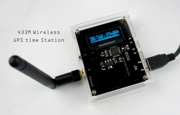
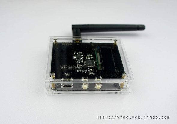
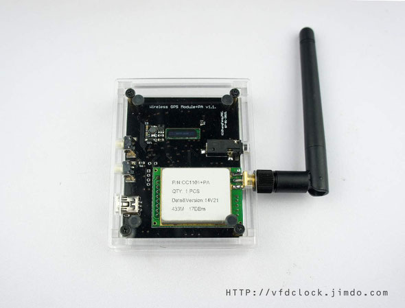
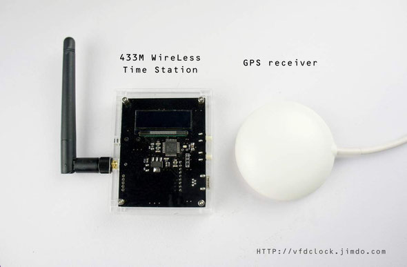
Mon
31
Aug
2015
KIT-Build a High Voltage power supply by using the MC34063 Chip

Please always download the Newest version of the PDF,the htm page may not be updated in time.
2. 8550 trans mark: [2TY] or [Y2];
older version
Build a High Voltage power supply
by using the MC34063 Chip
This kit allows you to make a MC34063 based boost PSU, which can accept a 12V DC input and output ~210V DC for powering NIXIE tubes and others that require high voltage. It is a very common circuit, the key point is the selection of the Inductor and the Mosfet.
Please do not change any equipments of the circuit or you may not be able to get the target HV output or the module may work under the lower efficiency state.
For more info & update, please visit HTTP://vfdclock.jimdo.com
Or contact us: zjjszhangf@gmail.com

How it works
The circuit is very simple, we used one of the most common switching regulators on the planet-the MC34063 chip. The circuit is the based on the Step-up structure. MC34063 contains a NPN output only structure, in order to drive the Mosfet, we add a 1K pull-down resistor(R2) to get the low side signal. And because we need to convert the 12V DC input to the ~210V DC output in one step, the ration requirement is very high, so we add a speed up circuit by using a PNP transistor(Q3) and a schottky diode(D2) to speed up the drop side of the driving wave. And in the current version, we added a ration jumper (X1), by connecting the different capacitors together, you can change the frequency of the circuit in High/Low levels, when the jumper shorted, you get lower frequency, which can get more higher ration, and more higher DC output even under heavy loader, but the efficiency of the circuit may have a little bit drop. Other part of the circuit is very simple, please check the MC34063 official PDF file by yourself.
Building it
Well, because of the circuit is pretty simple, all you need to do is get all the components in the right position and make sure no short before you plug the power. And the kit contains SMD components, so you must have the skills of soldering the SMD stuff. We will show the soldering steps and the matters needing attention blow.
1. Please print out the PCB installation diagram by yourself, the Circuit diagram is no need for soldering job, print it or not depends on you;
2. Check all the components in the kit bag, make sure nothing is missing (You can do it on a A4 white copy paper);
3. We recommend using a soldering station and small soldering tip for soldering this kit(we use F2 or CF2 type tip). If you have a hot air gun for soldering, that will be great. we recommend using ~180℃ soldering tin for this job. Please do not use the high temperature soldering tin in this project, you may damage a lot of SMD components;
Step 1:
Solder right-bottom part first, this part contains a R020 1206 resistor, a SOT-23 PMOSFET (X7HV), a 100nF/50V capacitor, and 3 frequency capacitor under the bottom (100pF/390pF/68pF), this step is very simple,just make sure the direction of the IC, do not go invert.

Step 2:
Solder the middle-right 2PCS 100uF/50V input capacitors(C1,C2 in 1206 package). These two capacitors are important part of the circuit, please solder carefully, use low temperature with no over 250℃ and solder fast, or you will lost the capacity or damage the capacitor. If possible, you can solder 3PCS of the cap by just solder the last one on the top of the other capacitor to get 300uF input capacity.(Note: Solder 2PCS 100uF cap at least, do not just solder 1PCS)
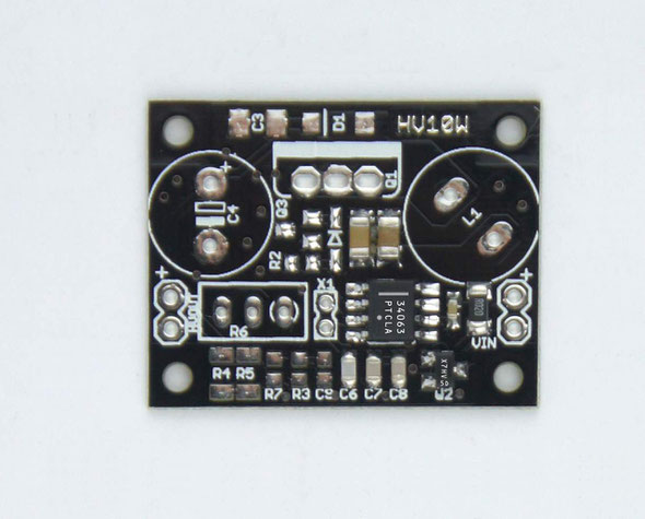
Step 3:
Solder the middle-left part, it contains R2,Q3 and D2(a IN4148 diode), those part are easy, just make sure the direction of the IN4148 diode is right, please check the picture blow.

Step 4:
Solder the top edge part, it contains C3 and D1, the C3 is a 0u1F/500V capacitor in 1206 package, if mixed with the 100uF capacitor that we used in the step 2, you can just measure the capacity by yourself, easy to find out. Also the D1 is the diode(usually be ES1J diode), take care of the direction too.
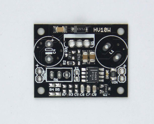
Step 5:
Solder the bottom-left part, it contains R4,R5,R7,R3,C6, the R7 and R5 are two 1M resistor in 1206 package, they are connected in serial in the circuit and been placed pretty close on the PCB, so please do short it. the R7(12K resistor in 0805/0603 package) is required for the HV feedback. the R3(51K resistor in 0805/0603 package) is for safety of the feed back circuit, please install it, and the C6(100pF/50V capacitor) is optional , we recommend you install it.
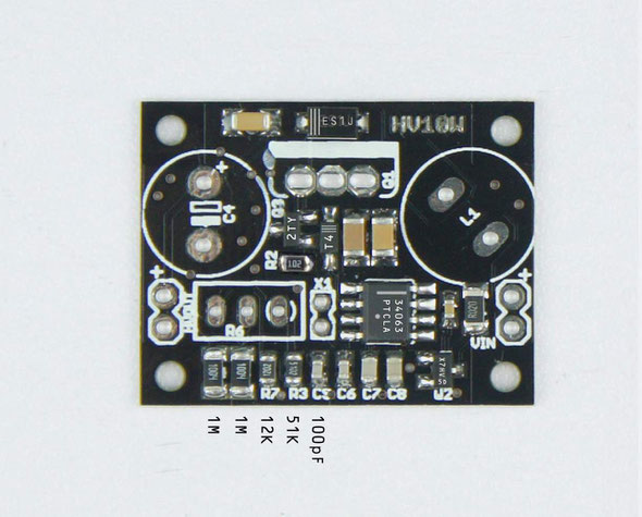
Step 6:
From step1~step5, we have finished soldering all the SMD parts of the circuit. Before we solder the DIP parts of the circuit, we can check the PCB and wash it first, after the PCB dried, you can cover it by using Plasticote(like CRC 70), or just escape this step.

Step 7:
Soldering all the DIP part of the circuit. The dip part contains L1,Q1,C4,R6,X1,PTH-IN,PTHOUT, those are easy part,
just take care of the C4(HV Aluminum Electrolytic Capacitor), it has polarity, do not install it in invert direction. And for the main HV mosfet (Q1), if the mosfet in the
kit is the TO220 package, you just need to plug it in the place, then cut the legs short and solder it, if the package is the TO263 package, band left&right legs straight by using needle-nose
pliers or other tools.

The mosfet's mark surface must be face the frond side of the PCB(face the MC34063 chip side).Double check the mosfet part after soldering, make sure it contains no short, it is very important!
The smoke test
Put the circuit board on an insulating surface, connect no loader to the output side, connect the input pin to a 9~12V DC source. If you have a current limited supply that will be perfect. Or you can try to use a 9V small home using MN1604 (6LF22) battery to prevent to burn something at the first time.
If all fine, the max output usually can go up to ~210V with no problem.
The whole circuit is pretty easy, no need to adjust.

Identifying the parts of your power supply kit
The following guide should help you to identify the parts and assemble it successfully
Resistors
All the resistors contains mark on one side of it's surface.
Diode
The diodes will be marked with ES1J(big one) and T4(the small one), the cathode side contains a few vertical line.
Capacitors
Kit contains two type of the 1206 size capacitors, one is 0u1/500V, the other is 100uF/50V, easy to find out by measure it. Other small size of the capacitors will have the make on the surface of its' package.
And for the Aluminum Electrolytic Capacitor, usually the longer lead is positive, or if both leads are the same, the negative is clearly marked with a big line or minus symbol running down the side of the case.
The MOSFET
The MOSFET will be marked 27N25 or other numbers, please note the mosfet marks surface must be installed face to the MC34063 chip side.
The MC34063 chip
MC34063 chip in this kit is SO8 package, make sure it is installed the correct way around, just follow the chip direction shown on the picture.
Partlist
Assembly variant:
|
Qty |
Value |
Device |
Parts |
Mark |
|
Resistors |
||||
|
1 |
R020 |
RESISTOR_EUR1206 |
R1 |
R020 |
|
2 |
1M |
RESISTOR_EUR1206 |
R4, R5 |
1004 |
|
1 |
1k |
RESISTOR_EUR0603/0805 |
R2 |
102 |
|
1 |
12k |
RESISTOR_EUR0603/0805 |
R7 |
1202 |
|
1 |
51k |
RESISTOR_EUR0603/0805 |
R3 |
5102 |
|
1 |
20k |
R-TRIMM3296W |
R6 |
203 |
|
Capacitor |
||||
|
1 |
68pF |
C-EUC0603/0805 |
C8 |
/ |
|
2 |
100pF |
C-EUC0603/0805 |
C6, C9 |
/ |
|
1 |
390pF |
C-EUC0603/0805 |
C7 |
/ |
|
1 |
0u1 |
C-EUC0603/0805 |
C5 |
/ |
|
2 |
100uF/50V |
C-EUC1206 |
C1, C2 |
/ |
|
1 |
0u1/500V |
C-EUC1206 |
C3 |
/ |
|
Diode |
||||
|
1 |
ES1J |
DIODE-SMA |
D1 |
ES1J |
|
1 |
T4 |
DIODE-SCHOTTKYSOD123 |
D2 |
T4 |
|
Trans/Mosfet/IC |
||||
|
1 |
X7HV |
P-OSFET |
Q2 |
X7HV-5D |
|
1 |
8550 |
PNP |
Q3 |
2TY |
|
1 |
34063 |
MC34063-SO8 |
IC1 |
34063PTCLA. |
|
PTH/Jumper |
||||
|
2 |
2.54mm PTH |
M02PTH |
HVOUT, VIN |
/ |
|
1 |
2mm PTH |
87758-0216 |
X1 |
/ |
|
1 |
2mm Jumper |
|
|
/ |
|
Others |
||||
|
1 |
100uH |
INDUCTANCE_US11X11PLUG |
L1-100UH |
/ |
|
1 |
Mosfet |
MOSFET-NCHANNELTO220V-BH2 |
Q1 |
/ |
|
1 |
3.3uF/400V |
CPOL-EUE5-10.5 |
C4 |
3.3uF 400V |
|
PCB |
||||
|
1 |
PCB |
|
|
|
exported from MC34063HV-02D-KIT
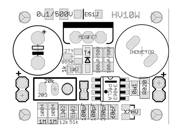
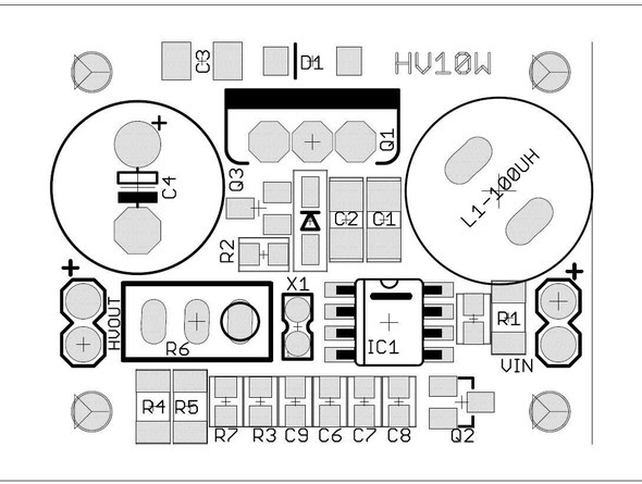
Sun
26
Jul
2015
OpenHardware-Pluggable-USB Powered IV-11 Single Digit VFD Tube Clock
Open Hardware Files:
Version 6.1.0 for Windows

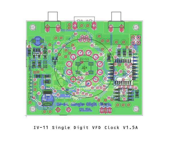
OpenHardware-Pluggable-USB Powered IV-11 Single Digit VFD Tube Clock
IV-11 Single Digit VFD Clock with acrylic enclosure
Brand new,I designed and made it by myself.
Product Change Notification in V1.5:
1.
Have moved the two buttons to the backside;
2. Have add the socket female pins on the PCB, which you can replace the tube by hand;
3. Update the RTC to DTCXO (temperature compensated crystal oscillator)
version, High Stability, Highly accurate.
It has ±1.9ppm (Equivalent to ±4.94s seconds of month deviation) under 0ºC~+40ºC. Usually you don't need to set the time for over a
year.

Specifications:
(For reference only)
Tube Name: IV-11 (Made in the U.S.S.R.)
Tube Size: 22.5mm(Dia.);
Tube Height: 60mm(no including the legs);
Digit Height: 21.0mm;
Digit Width:14.6mm;
Clock Supply: 5V DC via USB;
Working Current: <=250mA;
Clock Size: 54mm(L)*46mm(W)*70mm(H)
PCB Size: 44mm*36mm;
PCB Color: Black;
Weight: 43g(with the tube);
For home use only.
The clock works with any standard USB power supply,use only high-quality adapter!

Features:
(For reference only)
1).5V USB powered, easy to be used. Can connect to your computer's USB plugs directly.
2).Support 12H or 24H display modes, leading zero blanking is programmable.
3).Display date in all format: YY.MM.DD or DD.MM.YY or MM.DD.YY or even MM.YY.DD.
4).Support 3 different Effs : Normal/Fading/Cross Fading for displaying time.
5).High accuracy DTCXO RTC inside, ±1.9ppm, usually ±4.94 seconds (Max) per month. 6).Simple setting by using 2 buttons only and supports IR remote control.
7).Three alarms with weekends ON/OFF support, can be controlled individually.
8).Three programmable Auto Power ON/OFF mode, can turn ON/OFF tubes in any time you want. This function can save tubes life.
9).8-level adjustable tube bright with Auto-brightness feature(its ability to adjust the tube brightness depending on the current environment).
10). Rechargeable Backup Battery or Farad capacitor keeps RTC running during power outages.
11).Tri-colored RGB LED mounted under the tube. This LED can display any color with a lot of pre-defined auto color change effects.
12).Store user settings in non-volatile memory.
13).Beautiful CAD designed acrylic case made using a laser cutter makes the clock look beautiful. You can assemble/disassemble the case by using only 4 screws on the bottom of the case. The case also has 4 bumpers as feet on the bottom of the case in order to stop to prevent case's damage.

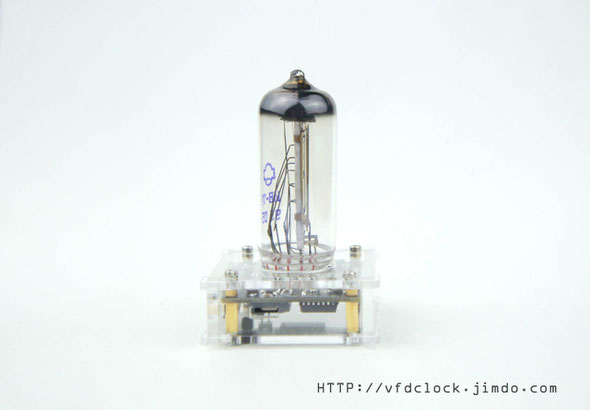
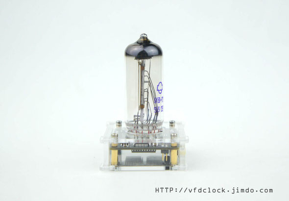

Sat
18
Jul
2015
Open Hardware-Highly Optimized-10W-MC34063 based High Voltage power supply module-High efficiency up to 85%-Small Size
New-10W-34063 Based High Voltage NIXIE&Magic Eye Tube Power
Supply Module
1.High power,up to 10W(Max) output;
2.High efficiency,up to 86.2%(Max);
3.Small
size,32mm(L)*26mm(W) only;
4.Open hardware design.
DANGER!
Lethal Potentials Present
LET ME CLARIFY FIRST:
THE USER IS WARNED THAT CAUTION MUST BE USED IN THE TESTING AND USE OF THE MODULE.
HIGH VOLTAGE, LETHAL POTENTIALS ARE PRESENT IN THIS MODULE. EXTREME CAUTION MUST BE USED IN WORKING WITH.
THIS MODULE CONTAINS DANGEROUS, HIGH VOLTAGE POTENTIALS. USE CAUTION.
DO NOT TOUCH ANY PART OF THE MODULE WHEN IT IS WORKING.
Tips:
1. Please control the input current in <=1A for the low heat working state,if need more power output,you can increase the input voltage;
2. Please use high quality and stable input DC source,make sure no over the MAX input voltage;
3. Module contains input reverse polarity protection;
4. For the heavy loader,the max output voltage may get drop,it's normal;
Description:
The HV10W series high voltage power converters are typical boost converters based on
34063 chip which can accept 9 to 18V DC input,and output up to ~210V DC(MAX) ,range set by an on-board 3296 trimmer resistor.
(For Lower DC input you get lower MAX DC output and for heavy loader you get
lower MAX DC output,read the details below).
eg: With 12Vin,under 10W output,the MAX HV output is about 180VDC;
This is a very common circuit,the key point of the circuit is the selection of the Inductor and the Mosfet.
The max efficiency is 86.2%, even under 12Vin, 10W output condition,the convert efficiency can still be ~84%.
The frequency is about 65KHz(If wanna try other freq,you can change the cap on-board by yourself.).
Typical Usage:
For driving NIXIE Tubes,Magic Eye Tubes and other applications requiring high DC
voltage.
Typical Parameters:
Input: 9V
DC~18V;
Output: 180V DC;
Max Power Output: 10W;(If increase the input voltage may get more power.)
Max efficiency: 86.2%;
Output setting: Adjustable with a single trimmer resistor;
Module size: 32mm(L)*26mm(W)*14mm(H); (*17mm(H) with TO220 type power mosfet been installed).
Frequency: ~65kHz;
Simple test by myself:
By using a KTEC 12V/1.5A AC Power Adapter which is for my WD USB HARD DRIVER,and driving a regular FSL 15W 220V~240V E14 light bulb,the results shown below:
Input: 12V;
Input Current: 980mA;
Output voltage: 180V with the light bulb turned on;
Output Current: 55mA;
Power output: 9.9W;
Efficiency: 84.18%;
No audible noise;
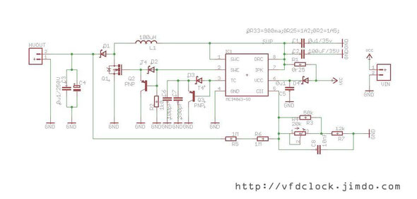

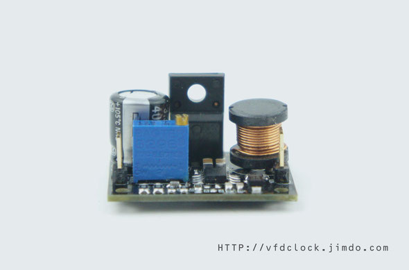
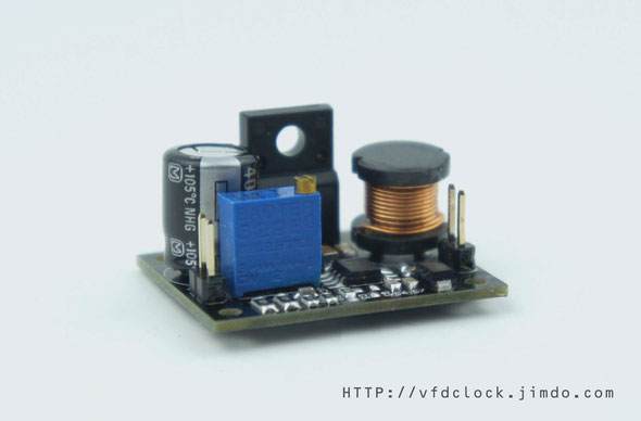

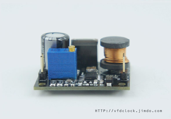
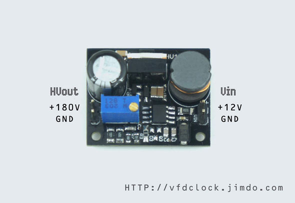
Wed
01
Jul
2015
New-HV12W PSU,5V~12V DC in,170V DC out,designed for driving 6-tube IN-18 NIXIE clock-92.6%(Max) high efficiency
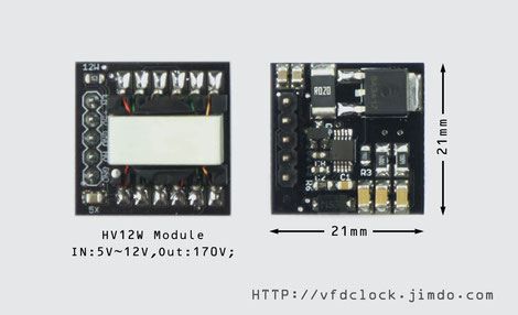
[Type C]-12Vin170Vout-HV12W-HIGH VOLTAGE NIXIE POWER SUPPLY MODULE
DANGER! Lethal Potentials Present
THIS MODULE CONTAINS DANGEROUS, HIGH VOLTAGE POTENTIALS. USE CAUTION.
DO NOT TOUCH ANY PART OF THE MODULE WHEN IT IS WORKING.
Newly designed,up to 92%(Max) high efficiency DC-DC converter for big tubes NIXIE clock.
When under 12V in for driving 6-tube IN_18 clock,you get almost no heat.
Max power output is 12W, enought for lighting up over 12PCS IN-18
NIXIE tubes together still with up to ~89% efficiency.
Product Change Notification :
Description:
1. This is a newly designed high voltage power converters;Can accept
5~12V DC in,and output ~170 DC;
2. Have increased the frequency up to about 200kHz to get more noiseless
output;
3. High quality transformer on-board to low down the noise;
4. It contains an ENABLE pin to turn the convert on/off,and can be controlled by an regular logic signal,like a MCU's GPIO PIN.
5. Module contains input reverse polarity protection and short protection circuit via current limiting.
6. No audible noise;
7. Standard 0.1"(2.54mm) pins, easy to be used, can use DuPont-Wires
etc.
Tips:
1.Please control the input current in <=1A for the low heat working state,if need more power output,you can increase the input voltage;
2.Please use high quality and stable input DC source,make sure the max input voltage is not over the max range;
3.We recommend using 12V as input;If using 5Vin,the module is still in working,but with low power output (<4W).
4.Do not go over power/Heat/voltage/current, will damage the MOSFET or IC or Transformer on
board.
Typical Usage:
For driving NIXIE Tubes and other applications which requir high DC voltage.
Typical Parameters:
(For reference only)
Input: 5~12V DC;
Output: ~170V DC
Max Power Output: 12W;(For working under 10W for 24*7
condition,the module get low heat.)
Max efficiency: 92.6%;
Module size: 21mm(L)*21mm(W)*10.5mm(H)---(16mm(H) including
the pins);
Module Pins : 0.1"(2.54mm) std. pins * 5;
PCB Color : Black;
Simple test by myself:
By using a KTEC 12V/1.5A AC Power Adapter which is for my WD USB HARD DRIVER,and driving a regular FSL 15W 220V~240V E14 light bulb(which I bought for my refrigerator early),the results shown below:
Input:12V, 820mA;
Output Voltage:169.5V with the light bulb turned on;
Output Current: 52mA;
Power output: 8.8W;
Efficiency: ~89.57%;
No audible noise;

Mon
29
Jun
2015
Pluggable-USB Powered IN-8-2 Single Digit NIXIE Tube Clock

Now we have the IN-8-2 Single Digit NIXIE clock Pluggable Version.
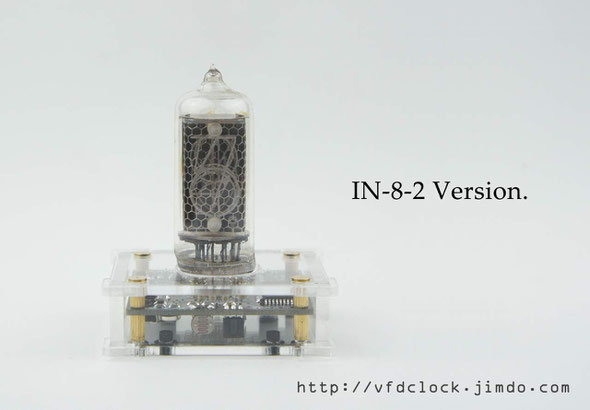
Mon
29
Jun
2015
Pluggable-USB Powered QS18-12 Single Digit NIXIE Tube Clock
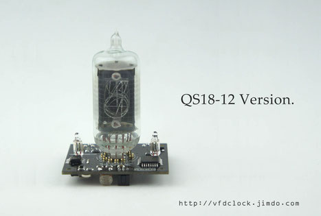
Pluggable - USB Powered QS18-12 SD NIXIE Tube Clock+Hard Legs Tube.
QS18-12 Single Digit NIXIE Clock with acrylic enclosure
Brand new,I designed and made it by myself.
Product Change Notification:
1.Update the RTC to DTCXO (temperature compensated crystal oscillator)
version,High Stability, Highly accurate.
It has ±1.9ppm (Equivalent to ±4.94s seconds of month deviation) under 0ºC~+40ºC. Usually you don't need to set the time for over a
year.
Specifications:
Tube Name:QS18-12(Made in the P.R.C.)
Tube Diameter:18mm;
Tube Height:40mm(approx including glass nipple);
Digit Height:15mm;
Clock Supply: 5V DC via USB;
Max Current: ~250mA;
Clock Size:50mm(L)*42mm(W)*70mm(H)
PCB Size:40mm*32mm;
PCB Color:Black;
Weight:~35g;
The clock works with any standard USB power supply,use only high-quality adapter!
Features:
1).5V USB powered,easy to be used. Can connect to your computer's USB plugs directly.
2). Support 12H or 24H display modes, can show "."as“A/P" in 12H time format.Leading zero blanking is programmable.
3). Display date in all format: YY.MM.DD or DD.MM.YY or MM.DD.YY or even MM.YY.DD.
4). Support 5 different Effs:Normal/Fading/Cross Fading/Slow Fading/Loop for displaying time.
5). High accuracy DTCXO RTC inside, ±1.9ppm, usually ±4.94 seconds (Max) per month.
6). Simple setting by using 2 buttons only and supports IR remote control(optional).
7). Three alarms with weekends ON/OFF support,can be controlled individually.
8). Three programmable Auto Power ON/OFF mode,can turn ON/OFF NIXIE tubes in any time you want.This function can save tubes life.
9). 8-level adjustable NIXIE tube bright with Auto-brightness feature(its ability to adjust the tube
brightness depending on the current environment).
10). Rechargeable Backup Battery or Farad
capacitor keeps RTC running during power outages.
11). Tri-colored RGB LED mounted under the NIXIE tube. This LED can display any color with a lot of predefined auto color change effects.
12). Store user settings in non-volatile memory.
13). Beautiful CAD designed acrylic case made using a laser cutter makes the clock look beautiful. You can assemble/disassemble the case by using only 4
screws on the bottom of the case.The case also has 4 bumpers as feet on the bottom of the case in order to stop to prevent case's damage.


Thu
04
Jun
2015
10W-120kHz High Voltage Supply Module-Designed for Audio Amplify Circuit
15W ~120kHz High Voltage Supply Module

[TYPE A]-High Freq-220V High Voltage Power Supply Module,Power Supply
Module Std.
DANGER! Lethal Potentials Present
THIS MODULE CONTAINS DANGEROUS, HIGH VOLTAGE POTENTIALS. USE CAUTION.
DO NOT TOUCH ANY PART OF THE MODULE WHEN IT IS WORKING.
Description:
1. This is a newly designed high voltage power converters;Can accept 9~18V DC in,and output up to about 220V DC,range set by an on-board 3296 trimmer resistor(For Lower DC input you get lower
MAX DC output).
2. Have increased the frequency up to about 120kHz to get more noiseless output to suit for the Audio amplifying
circuit etc;
3. High quality transformer customized by factory with two shield layers inside to low down the noise;
4. It contains an /ENABLE pin to turn the convert on/off,and can be controlled by an regular logic signal,like a MCU's GPIO PIN.
5. No audible noise;
6. Standard 0.1"(2.54mm) pins, easy to be used, can use DuPont-Wires etc.
Tips:
1.Please control the input current in <=1A for the low heat working state,if need more power output,you can increase the input voltage;
2.Please use high quality and stable input DC source,make sure the max input voltage is not over the max range;
3.For the heavy loader,the max output voltage may get a little bit drop,it's normal;
4.If needed,you can add an LC filter on the audio board by yourself;
5.Do not go over power/Heat/voltage/current, will damage the MOSFET or IC or Transformer on board.
Typical Usage:
For driving Audio AMP/NIXIE Tubes/Magic Eye Tubes and other applications requiring high DC
voltage.
Typical Parameters:
(For reference only)
Input: 12V DC;
Output: 200V DC
Max Power Output: 10W;(For working under 10W for 24*7
condition,please take care of the mosfet's temperature,do not go over-heat.)
Max efficiency: 86.2%;
Output setting: Adjustable with a single trimmer resistor;
Module size: 45mm*33mm*13mm;
Simple test by myself:
By using a KTEC 12V/1.5A AC Power Adapter which is for my WD USB HARD DRIVER,and driving a regular FSL 15W 220V~240V E14 light bulb(which I bought for my refrigerator early),the results shown below:
Input:12V;
Output Voltage:190V with the light bulb turned on;
Output Current:53mA;
Power output:~10W;
Efficiency:83.9%;
No audible noise;
Worked fine under 24*7 condition,the max MOSFET temperature is about 65℃(degree C).
------------------------------------------------------------------------------------------------------
Output 230V 65mA output,Wout=15W;
(For testing only,do not work under this condition).
The Module can work,but after 2
hours,the mosfet over heat and been damaged.
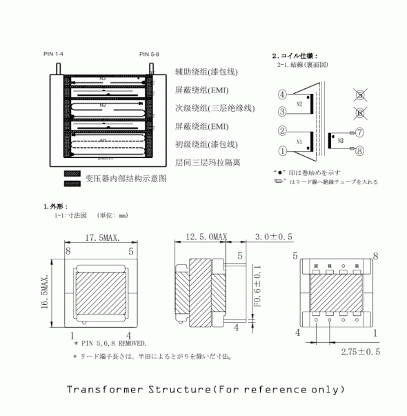


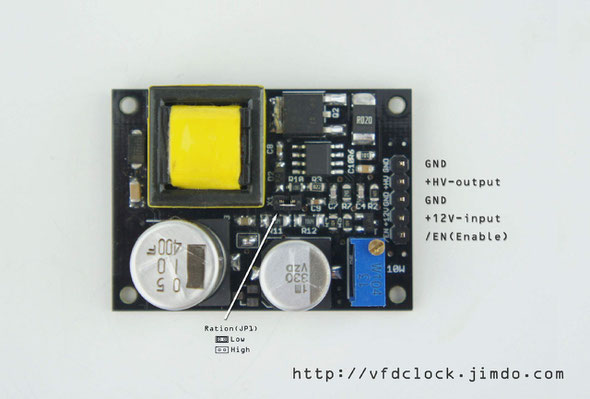
Mon
25
May
2015
92% efficiency High Voltage Power Supply Module-15W
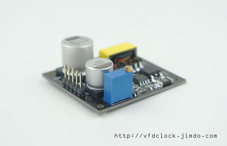
92% High efficiency High Voltage Power Supply Module
Brand New Design,High Frequency,High Power,Hig Efficiency.
Just tested by myself,under 10W output,working in 24*7 condition,the module got almost no heat!
More info will come soon.
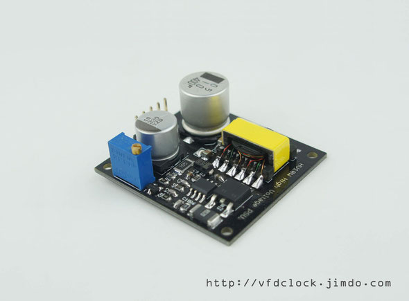
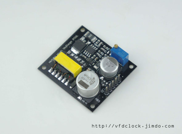

Mon
25
May
2015
Open Hardware-MC34063 based High Voltage Power Supply Module-10W
MC34063 based High Voltage Boost Power Supply Module
This is a very common circuit,the key point of the circuit is the selection of the Inductor and the Mosfet.
The Module can output 10W power and the max efficient is 85%, even under 12Vin,10W output condition,the convert efficient still be no less than 75%.
The frequency is about 30KHz, no audible sound.


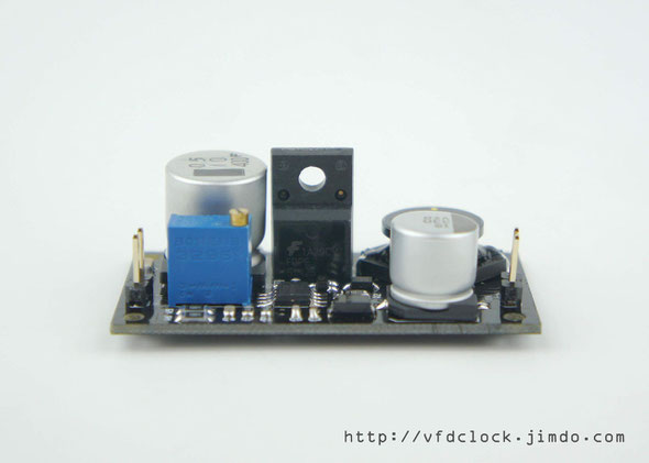

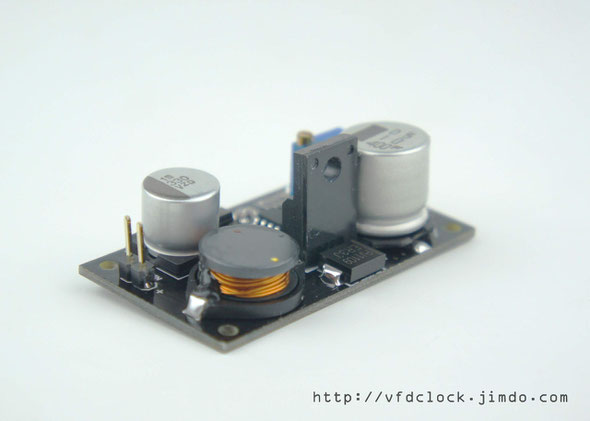
Fri
08
May
2015
Open Hardware - GPS Receiver Module for NIXIE/VFD clocks
In order to add the GPS time base synchronization function for our NIXIE/VFD clocks, we designed this GPS Receiver Module and created with high quality components and the ABS enclosure we customized from the factory, instead of using the low quality GPS module in the market.
This GPS Receiver Module is open hardware, we provide Eagle Source file, gerber file, and all the datasheets we have. We also provide a simple Source Code for ARDUINO for parsing the GPS data.
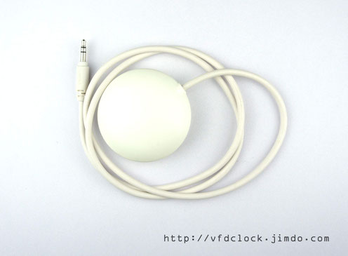
Features:
- Compass GPS module;
- Active antenna inside, with fast satellite searching speed and high precision;
- NMEA protocol output in default;
- UART TTL serial output in 4800bps;
- High quality white round plastic shell;
- With LED indicate for GPS status;
- 3.5mm stand Mini Phono Plug;
- Open Hardware and Source code for ARDUINO;
The Sample output from the GPS module:
$GPGGA,005350.000,2655.5236,N,18838.6134,E,1,06,1.9,93.9,M,5.8,M,,0000*55
$GPGSA,A,3,15,24,12,18,22,14,,,,,,,3.2,1.9,2.5*31
$GPGSV,3,1,11,18,73,168,30,22,66,302,31,25,50,141,25,12,44,079,39*7F
$GPRMC,005350.000,A,2655.5236,N,18838.6134,E,0.00,,050515,,,A*7D
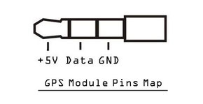

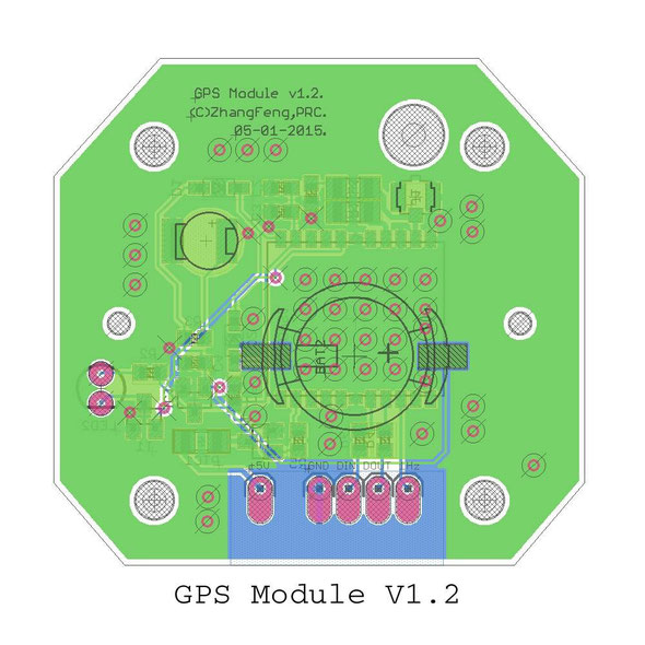


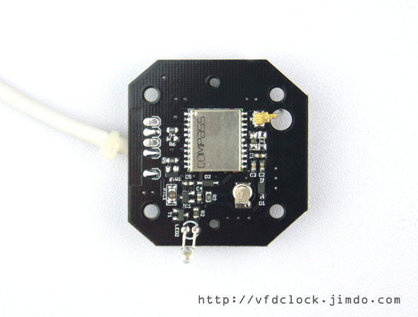

Sat
07
Mar
2015
NEW-Plug&Play IN-14 6-tube NIXIE Clock V1.2
This is our brand new design of the IN-14 6-tube NIXIE clock v1.2.
We call it "A Giant Leap"!!!
New module based structure,also USB powered,add socket pins which we customized from the fatory.
Now all the IN-14 NIXIE tubes and the middle dot-bulbs can be replaced by hand directly, you don't need any tools.
All the NIXIE funs now no need to worry about the tubes' life of this clock.
Add 5 dots effects....
More info will coming soon.


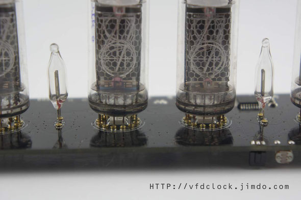
Tue
10
Feb
2015
VFD48 Round VFD Module For ARDUINO/51/AVR/STM8S/STM32 etc.
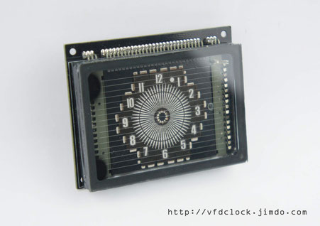
You can find PDF password inside your parcel.
For the VFD48-1202Fn panel datesheet,Visit:
http://vfdclock.jimdo.com/2013/02/02/vfd-flat-screen-datasheet-archive/

How to connect 5V VFD48 Module with 3V3 MCU
Specifications:
Panel
Name: BOE VFD48 (Made in the P.R.C.);
Panel Size: :68mm(L)*48mm(W)*8.5mm(T);
Module Supply: 5V DC via Arduino or USB;
Working Current: ~200mA;
Module Size:70mm(L)*55mm(W)*15mm(H);
PCB Size:70mm(W)*55mm(H);
PCB Color: Black;
Weight:56g;
The vfd48 module also works with STM8S/STM32/PI/51/AVR etc.;
The module works with any 5V DC MCU, especially designed for ARDUINO!
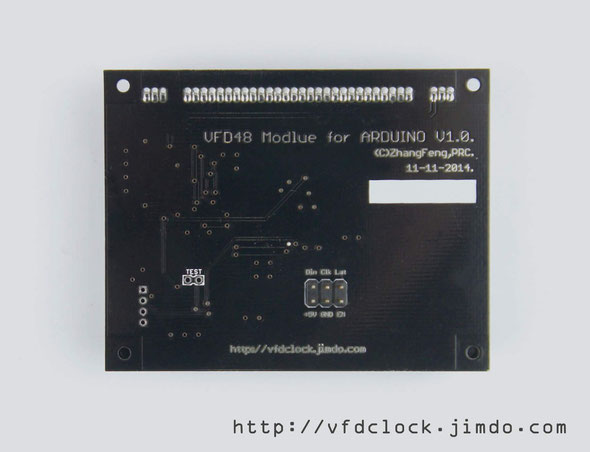
Features:
1). 5V Ready, easy to be used. Can connect to your ARDUINO UNO board with only 3 signal wires;
2). High efficiency power circuit, no transformer, no heat, Low HV, very safe, High Brightness;
3). All SMT components, very thin PCB, easy to drive;
4). All segments in the VFD panel can be lighted up;
5). Module contains a self-test jumper, when shut the jumper and then plug the power on, the module will enter the self-testing module, no need other MCU, easy to check module's condition;
6). Contains over-current protection, and reverse connection protection circuits;
7). Open source ARDUINO NUO source code, pure C code, provide high level function, easy to be used;
9). Simple 3-wire SPI interface, with EN pin, support adjusting the global brightness and shutdown the High Voltage and Filament Supply completely.
Interface:
3-wire SPI:
+5V
GND
DIN
CLK
LATCH(STROB)
EN - (optional)High voltage & filament supply enable
Std. 0.1”(2.54mm) 2*3Pins;


Tue
27
Jan
2015
New-HV5W NIXIE High Voltage Module,5V DC in,170V DC out
This Module is newly design,which can light up about 10PCS IN-14 NIXIE tubes with 10k resistor in serial under the 5V DC in.
Now all of NIXIE fans can use the 5V USB power to drive the NIXIE clocks.
Module is pretty small,and with high eff,the module got almost no heat.
More pictures will be added soon.
NEW-Small HV5W HIGH VOLTAGE NIXIE POWER SUPPLY MODULE PSU-NIXIE TUBE ERA
DANGER! Lethal Potentials Present
THIS MODULE CONTAINS DANGEROUS, HIGH VOLTAGE POTENTIALS. USE CAUTION.
DO NOT TOUCH ANY PART OF THE MODULE WHEN IT IS WORKING.
Tips:
1. Standard 0.1"(2.54mm) pins, easy to be used, can use bread board or DuPont-Wires etc.
2. Please control the input current <=800mA for the low heat working state;
3. Module contains input reverse polarity protection and over current protection. When over heat, the module will turn off, you need to re-power on to reset the module;
4. Please use high quality and stable input DC source, do not go over voltage;
5. For the heavy loader, the max output voltage may get a little bit drop;
6. If one module's power is not suited for your app,use two or more modules for driving the seperated NIXIE tube(s) group,etc.;
7. Do not connect the modules' outputs in "Parallel Connection"!!!
Description:
HV5W is a newly designed high voltage module,
it works under 5V USB power, with ~170V
DC output, especially designed for driving the NIXIE tubes. The max power output is enough for lighting up 6PCS IN-14 NIXIE tubes + 4PCS NE-2 neon bulbs. Low EMI and with No audible noise.
It contains an ENABLE pin to turn the module on/off, and can be controlled by an
regular logic signal, like a MCU's GPIO PIN.
We use the same module in our new "6-Tube IN-14 Clock" design, the prototype has been working for over 2 month under 24*7 condition, the clock worked fine, and the module got
almost no heat.

Specifications:
Module Size : 18mm*16mm;
Module Pins : 0.1"(2.54mm) std.
pins;
PCB Color : Black;
Pin Functions
|
ID |
Name |
Description |
|
0 |
EN |
Enable pin for turning the module ON/OFF(Optional) |
|
1 |
Vcc/+5V |
Input supply voltage, 4V5 to 7V5.(Recommend 5V) |
|
2 |
GND |
Ground |
|
3 |
HV |
High voltage output. +170V(+-5%) |
|
4 |
GND |
Ground(Optional) |
* You can use the middle 3 pins only.
For 24*7 continually working condition, we recommend you control the input current less than 800mA when under 5V in, it keeps this module working under the low heat condition.
And this module is also suite for driving 6 tubes IN-18 clock, you just need to use two modules for driving it. Each module can drive 3PCS IN-18 tubes + 2PCS NE-2 neon bulbs (as dots) with no problem.
Typical Usage:
For driving NIXIE Tubes;
Simple testing by myself:
By using the 5V/1A5 USB Power Adapter as the input DC source, we tried to light up some NIXIE tubes:
1. No load, the HV output=170.6V;
2. Lighting up 6PCS IN-14 tubes, the HV output=166.2V; Worked fine in 24*7 condition.
3. Lighting up 3PCS IN-18 tubes, the HV output=164.6V; Worked fine in 24*7 condition.
No audible noise;
4. Lighting up 6PCS IN-18 tubes (For testing only.) (All with number
"8" been lighted up), the HV output=162.5V, all the tubes can be lighted up in high brightness. After working for few minutes, the module goes heat, the input current keeps increasing slowly,
after the input current went over about 1A3, the module entered the protection mode.
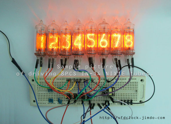
The data shown below is for reference only!!!
Absolute Maximum Ratings
|
Parameter |
Symbol |
Value |
Unit |
|
Input Voltage |
Vin(Low) |
4.5 |
V |
|
Output Voltage |
Voutput |
178 |
V |
|
Output Power |
Poutput |
5 |
W |
Electrical Characteristics (DC Parameters)
|
Parameter |
Symbol |
Test Condition |
Min. |
Typ. |
Max. |
Unit |
|
Input operation voltage |
Vin |
/ |
4.5 |
5 |
7.5 |
V |
|
Output Voltage |
Voutput |
/ |
160 |
170 |
175 |
V |
|
Output Current |
Ioutput |
Vin=5V, |
0 |
15 |
20 |
mA |
|
No Load Current - |
Inoload |
Vin=5V |
10 |
15 |
20 |
mA |
|
Efficiency |
η |
Vin=5V, |
65.0 |
80.5 |
88.6 |
% |
|
EN Pin Threshold |
VEN |
High(Regulator OFF) |
|
1.2 |
|
V |
Notes:
1. En pin = high (default) will turn the module on.
2. Module contains input reverse polarity protection.
3. Module contains over current protection circuit, when over power or over heat it will turn off the HV output, you need to re-power on to rest the
module.
Fri
16
Jan
2015
Pluggable - USB Powered IN-14 SD NIXIE Tube Clock+Hard Legs Tube.
Pluggable - USB Powered IN-14 SD NIXIE Tube Clock+Hard Legs Tube.
Specifications:
Tube Name:IN-14(Made in the U.S.S.R.)
Tube Diameter:18mm;
Tube Height:55mm(approx including glass nipple);
Digit Height:17mm;
Digit Width:10mm;
Clock Supply: 5V DC via MINI-USB;
Max Current: ~250mA;
Clock Size:50mm(L)*42mm(W)*70mm(H)
PCB Size:40mm*32mm;
PCB Color:Black;
Weight:38g;


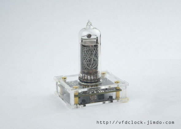

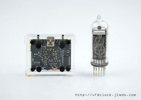
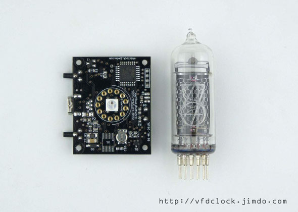
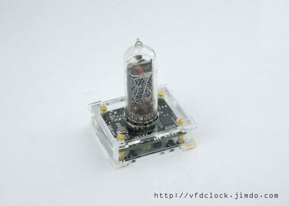
Thu
15
Jan
2015
Customized the NIXIE PINS from the factory,1U gold plated,Very high quality
Just got the customized NIXIE PINS from the factory,1U gold plated,just manufactured in Jan-05-2015,Bright and Shining,Very High Quality;

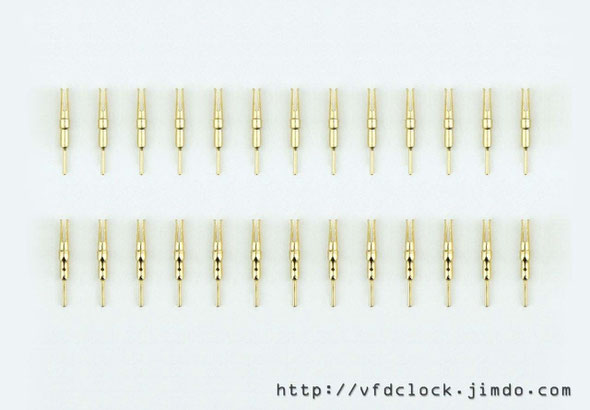
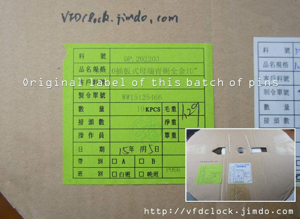
Tue
28
Oct
2014
USB Powered 6E1P(EM80) Magic Eye VU Meter(Audio Visualizer)-V1.0
USB Powered 6E1P (EM80) Magic Eye VU Meter(Audio Visualizer) -V1.0
Consumer Electronics > Gadgets & Other Electronics > Other
Brand new, I designed and made it by myself.
Specifications:
Tube Name: 6E1P(EM80);
Power Supply: 5V DC via MINI-USB;
Working Current: ~500mA;
Size: 58mm(L)*50mm(W)*80mm(H) ( with the tube installed);
PCB Size: 48mm(L)*40mm(W);
PCB Color: Black;
Weight: 50g(with the tube);
The 6E1P VU-meter works with any standard USB power supply, use only high-quality adapter!
Caution: High Voltage inside! For indoor use only!
Features:
1).5V Mini-USB powered, easy to be used. Small size, high efficiency. Can connect to your computer's USB plugs directly.
2).Round trimmer resistor installed on the right side of the case, easy for adjusting the circuit's sensitivity;
3).Tri-colored RGB LED mounted under the tube. This LED can display any color with a lot of pre-defined colors as back light;
4).Simple setting by using 1 button only, can Turn ON&Turn Off the power and switch the LED's color or turn off the LED;
5).The tube is installed in the Gold Plated Stamped Contacts. you can replace tube by yourself without using any tools;
6).Support 3.5mm Line_in and MIC (optional) on board, and also has a 3.5mm Line_out socket installed, you can just connect the VU-meter to your computer's sound output or other sound source and connect your headphone to the VU-meter;
7).Beautiful CAD designed acrylic case made using a laser cutter makes the clock look beautiful. You can assemble / disassemble the case by using only 4 screws on the bottom of the case. The case also has 4 bumpers as feet on the bottom of the case in order to stop to prevent case's damage.
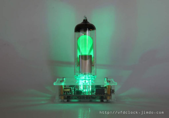
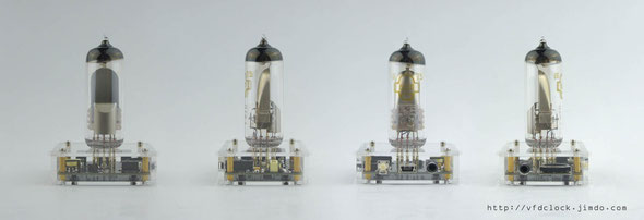
It must be very interesting if the 6E1 is put next to the 6E2 and let them display their own patterns with the same music. I bet the 6E1 will be more outstanding. I am looking forward to see this 6E1 module to be appeared in your taobao shop soon!
Sat
23
Aug
2014
USB Powered 6-Tube IN-14 NIXIE clock V1.0-USB供电的IN-14辉光管时钟

USB Powered IN-14 6-Tube Digit NIXIE Tube Clock V1.0.
IN-14 6-Tube Digit NIXIE Clock with acrylic enclosure
Brand new,I designed and made it by myself.
Notice:
In order to drive the NIXIE tube, some internal equipments are under the High Voltage(up to 180V DC),please do not use this clock outside or in any wet
conditions,please do not touch any part inside the clock when power supply is turned on.Always keep it away from kids.
Specifications:
Tube Name: IN-14(Made in the U.S.S.R.)
Tube Diameter: 18mm;
Tube Height: 55mm (approx including glass nipple);
Digit Height: 17mm;
Digit Width: 10mm;
Clock Supply: 5V DC via MINI-USB;
Max Current: <=850mA;
Clock Size: 210mm (L)*56mm(W)*15mm(H)(*68mm(H)with IN-14 tube installed);
PCB Size: 186mm*45mm;
PCB Color: Black;
Weight: 218g;
The clock works with any standard USB supply,use only high-quality
adapter!
Features:
1).5V Mini-USB powered, easy to be used. Can connect to your computer's USB plugs directly (*In some computers you may need to use the USB Cable that Have Two USB Connectors at the End.).
2).High efficiency circuit and separated HV supply structure make the Clock less heat and very safe. We use 7 individual small transformers to drive the 6 tubes and 4 middle dots, each provides 3mA Max HV power output only which is pretty safe than regular one HV DC-DC supply solution;
3).All SMT components, very thin PCB, only 8mm(max)
high with the Top & Bottom components; Static driving, No Blue Dot, No Flashing, High Brightness;
4).Support 12H or 24H display modes, can show "." as "A/P" in 012H time format. Leading zero blanking is programmable.
5).Display date in all format: YY.MM.DD or DD.MM.YY or MM.DD.YY or even MM.YY.DD; Can display week info too.
6).Support 7 different Effects: Normal/ Fading/ Cross Fading/Slow Fading /Flash /Loop /Random
Loop for displaying time. All the segments in the IN-14 tube can be lighted up, include the Left & right dots;
7).High accuracy RTC inside, factory calibrated to ± 5ppm,±13 seconds (Max)per month.
8).Simple setting by using 3 buttons only and supports IR remote control (optional).
9).Three alarms with weekends ON/OFF support can be controlled individually.
10).Three programmable Auto Power ON/OFF mode, can turn ON/OFF NIXIE tubes in any time you want. This function can save tubes life.
11).8-level adjustable NIXIE tube bright with Auto-brightness feature (its ability to
adjust the tube brightness depending on the current environment).
12).Rechargeable Backup Battery or Faradcapacitorkeeps RTC running during power outages.
13).Tri-colored RGB LED mounted under the each NIXIE tube. These LEDs can display different colors at the same time, with a lot of
pre-defined auto colour change effects.
14).Store user settings in non-volatile memory.
15).Beautiful CAD designed acrylic case made using a laser cutter makes the clock look beautiful. You can assemble/disassemble the case by
using only 4 screws on the bottom of the case. The case also has 4 bumpers as feet on the bottom of the case in order to stop to prevent
case's damage.
16).Can install Temperature Sensor(optional) ;Can
install 433M wireless module(optional) for receiving
the outside info, like the wireless temperature sensor's data and the GPS time sync data, etc.

全新USB供电的前苏联IN-14六管辉光时钟 秒杀国产QS1-12
Brand new,I designed and made it by myself.
注意事项Notice:
辉光管为高压驱动设备,内部包含180V直流高压,请勿在室外或者潮湿的环境下使用,请勿让儿童接触使用;
In order to drive the NIXIE tube, some internal equipments are under the High Voltage(up to 180V DC),please do not use this clock outside or in any wet conditions,please do not touch any part inside the clock when power supply is turned on.Always keep it away from kids.
产品规格Specifications:
显示管名Tube Name:IN-14(前苏联制造Made in the U.S.S.R.);
显示管直径Tube Diameter:18mm;
显示管高度Tube Height:55mm(包含顶部玻璃气嘴approx including glass nipple);
数字高度Digit Height,:17mm;
数字宽度Digit Width:10mm;
电源Clock Supply: 5V DC via MINI-USB;
最大工作电流Max Current: <=850mA;
产品尺寸Clock Size:210mm(L)*56mm(W)*15mm(H)(*包含显示管高度为68mm(H));
印刷电路板尺寸PCB Size:186mm*45mm;
印刷电路板颜色PCB Color:黑色Black;
产品重量Weight:218g;
时钟可使用任何5V/1A的USB电源适配器驱动,请一定使用优质的电源适配器!(实际测试情况表明市场上目前的“PALM小猪头”可以稳定驱动)
The clock works with any standard 5V/1A USB power supply,use only high-quality adapter!
功能特性Features:
1). 5VMini-USB电源供电,可直接与USB口连接(*部分电脑可能需要使用双头供电的USB线,以确保电流供应);
1).5V Mini-USB powered,easy to be used. Can connect to your computer's USB plugs directly(*In some computers you may need to use the USB Cable that Have Two USB Connectors at the End.).
2).高效的高压升压电路,低发热,高安全性;本制作使用7只独立的微型变压器实现驱动6只IN-14管及冒号氖灯,每组高压最高输出电流控制在3mA,远比单一高压升压方案来的安全;
2).High Eff circuit and seperated HV supply structure make the Clock less heat and very safe.We use 7 individual small transformers to drive the 6 tubes and 4 middle dots,each provides 3mA Max HV power output only which is pretty safe than regular one HV DC-DC supply solution;
3).全贴片元件,PCB连同上下板元件总高度不超过8mm,超薄设计;全静态高压驱动方案,确保无蓝点,显示无闪烁,高亮度;
3).All SMT components,very thin PCB,only 8mm(max) hight with the Top&Bottom components;Static driving,No Blue Dot,No Flashing,High Brightness;
4).支持12小时与24小时时制,支持以[.]号表示"AM/PM",支持开启或关闭前导零功能;
4).Support 12H or 24H display modes, can show "." as "A/P" in 012H time format.Leading zero blanking is programmable.
5).支持以所有可能的四种顺序显示日期;
5).Display date in all format: YY.MM.DD or DD.MM.YY or MM.DD.YY or even MM.YY.DD;Can display week info too.
6).支持七种时间显示切换方式:普通切换/渐变切换/交叉渐变切换/慢速渐变切换/闪切/循环切换/随机循环切换;所有六只IN_14辉光管的0~9显示字符及左右点号都可以独立点亮;
6).Support 7 different Effs:Normal/Fading/Cross Fading/Slow Fading/Flash/Loop/Random Loop for displaying time.All the segs in the IN-14 tube can be lighted up,includ the Left&right dots;
7). 高精度时钟,± 5ppm工厂预校正晶体,每月最大误差在±13秒以内;
7).High accuracy RTC inside, factory calibrated to ± 5ppm,±13 secons(Max)per month.
8).本机三按键操作,同时支持红外遥控器(可选,橡胶按键,手感好);
8).Simple setting by using 3 buttons only and supports IR remote control(optional).
9).提供三组独立的闹铃设置,支持周末闹铃关闭功能;
9).Three alarms with weekends ON/OFF support,can be controlled individually.
10).提供三组独立的自动开关机设置,此功能可提高NIXIE管的使用寿命;
10).Three programmable Auto Power ON/OFF mode,can turn ON/OFF NIXIE tubes in any time you want.This function can save tubes life.
11).8级可调的整体亮度设置,同时支持自动环境光检测功能;
11).8-level adjustable NIXIE tube bright with Auto-brightness feature(its ability to adjust the tube brightness depending on the current environment).
12).内置可充电电池或法拉电容作为RTC后备供电,可确保长时间断电走时;
12).Rechargeable Backup Battery or Farad capacitor keeps RTC runing during power outages.
13).管子下方的六只真彩色RGB LED各自独立,可显示任意色彩,具备呼吸灯效果及多种内置的色彩切变效果;
13).Tri-colored RGB LED mounted under the each NIXIE tube. These LEDs can display different colors at the same time,with a lot of pre-defined auto colour change effects.
14).用户的设置被保存在内部EEPROM内,断电后无需重新设置;
14).Store user settings in non-volatile memory.
15).CAD设计及激光切割的全透明亚克力外壳,仅使用底部的四颗螺丝即可完成组装;外壳底部同时包含4只进口硅胶脚垫,确保摆放稳定,同时可防止刮花外壳或桌面;
15).Beautiful CAD designed acrylic case made using a laser cutter makes the clock look beautiful. You can assamble/disassamble the case by using only 4 screws on the bottom of the case.The case also has 4 bumpers as feet on the bottom of the case in order to stop to prevent case's damage.
16). 可选DS18B20作为温度传感器(可选件,未包含在本产品内);可安装433M无线接收模块(可选件),以实现接收无线温度湿度传感器及GPS时间同步信号等功能;
16).Can install Temperature Sensor(optional) ;Can install 433M wireless module(optional) for receiving the outside info,like wireless temperature sensor's data and the GPS time sync data,etc.
Sun
17
Aug
2014
IN-18 Nixie Module for ARDUINO 为ARDUINO设计的IN-18辉光模块
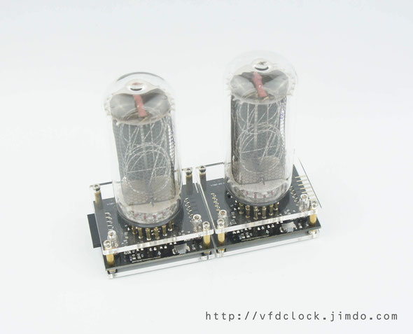
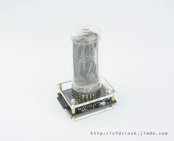
Sun
17
Aug
2014
New-HV15W High Voltage NIXIE and Magic Eye Tubes PSU,Power Supply Module V1.0 Std.-MAX1771 Version
This module is referenced from the MAX1771 based "Nixie HV Switching PSU" from:
http://desmith.net/NMdS/Electronics/NixiePSU.html
The Datasheet of MAX1771:
http://pdfserv.maximintegrated.com/en/ds/MAX1771.pdf
EAGLE (Easily Applicable Graphical Layout Editor) Version 6.1.0 for Windows;
Note:
The data is for reference only;
We have tested the MAX1771CSA and the MAX1771ESA,all worked fine.
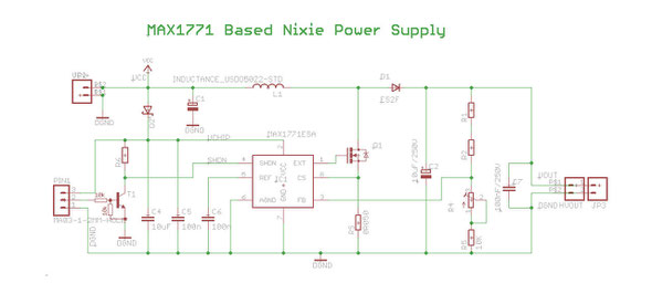
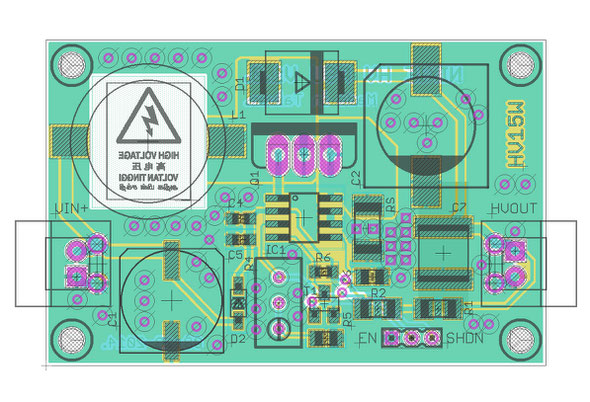

New-HV15W High Voltage NIXIE and Magic Eye Tubes PSU,Power
Supply Module Std.
DANGER! Lethal Potentials Present
LET ME CLARIFY FIRST:
THE USER IS WARNED THAT CAUTION MUST BE USED IN THE TESTING AND USE OF THE MODULE.
HIGH VOLTAGE, LETHAL POTENTIALS ARE PRESENT IN THIS MODULE. EXTREME CAUTION MUST BE USED IN WORKING WITH.
THIS MODULE CONTAINS DANGEROUS, HIGH VOLTAGE POTENTIALS. USE CAUTION.
DO NOT TOUCH ANY PART OF THE MODULE WHEN IT IS WORKING.
Product Change Notification in the New Version:
1.Module contains input reverse polarity protection;
2.Small size,and update the output cap to 10uF/400V(Sanyo);
3.Add 4 install mounting holes;
4.Able to install 2.54mm std 2-pin at the input & output parts;
Description:
The HV15W series high voltage power converters are typecial current mode boost
converters which can accept 9 to 24V DC input,and output of 85 to 220V DC range
set by an on-board 3296 trimmer resistor(For Lower DC input you get lower MAX DC output,read the details below).
It contains an ENABLE pin to turn the convert on/off,and can be controlled by an regular logic signal,like a MCU GPIO PIN.
No audible noise,intsead of NE555/MC34063 style PSU;
Typical Usage:
For driving NIXIE Tubes,Magic Eye Tubes and other applications requiring high DC
voltage.
Typical Parameters:
Input:12V DC;
Output:175V DC;
Max power:15W;
Max efficiency:88.6%;
Output setting:Adjustable with a single trimmer resistor;
Module size: 49mm*32mm*15mm(DC headers are not included);
Simple test by myself:
By using a KTEC 12V/1.5A AC Power Adapter which is for my WD USB HARD DRIVER,and driving a regular FSL 15W 220V~240V E14 light bulb(which I bought for my refrigerator early),the results shown below:
Input:12V;
Max output voltage:185V with the light bulb turned on;
Power output:9W;
Efficiency:86.6%;
No audible noise;
Note:
This module is especially designed for driving NIXIE tubes from 12V DC to 175V
DC,and you can get more higher voltage by increasing the input voltage,with a 16V DC input or higher ,you can get 220V max DC output.For the Circuit and PCB files in Eagle Cad format,you can visit my
website:
We may not be able to provide extra technology support!
We may will change the Circuit/PCB/Components without notification!
Contains:
1PCS HV15W power supply module with DC headers,ready to go.(without any tubes,without power
adapter,without wires;)
Payment methods:
We ONLY accept PayPal on eBay
selling, other payment is not acceptable.
Please PAY within 7 days, or we'll re-selling the item.
Shipping:
We ship to American via ePacket delivery with tracking number;
We ship to other countries/locations via International Enconomy Package by CHINA POST with tracking number;
Shipping time:10-20 working days for ePacket Delivery to the U.S.A.(normally you will receive it in
about two weeks), depends on the destination location;For other far locations it may need more days.
We ship to your PAYPAL Verified Address only;
Any import tax or charges should be paid by the
buyer.
=====================================================================================
The data shown below is for reference only!!!
Absolute Maximum Ratings
|
Parameter |
Symbol |
Value |
Unit |
|
Input Voltage |
Vin(Low) |
9 |
V |
|
Output Voltage |
Voutput |
250 |
V |
|
Output Power |
Poutput |
25 |
W |
Electrical Characteristics (DC Parameters)
|
Parameter |
Symbol |
Test Condition |
Min. |
Typ. |
Max. |
Unit |
|
Input operation voltage |
Vin |
|
9 |
12 |
24 |
V |
|
Output Voltage |
Voutput |
|
70 |
180 |
220 |
V |
|
Output Current |
Ioutput |
Vin=12V, |
0 |
50 |
70 |
mA |
|
No Load Current - |
Inoload |
Vin=12V |
10 |
15 |
20 |
mA |
|
Efficiency |
η |
Vin=12V, |
78.0 |
86.5 |
88.0 |
% |
|
EN Pin Threshold |
VEN |
High(Regulator OFF) |
|
1.2 |
|
V |
Notes:
1.Short the ENABLE jump can turn the module off.
2.Module contains input reverse polarity protection.
3.Module contains short protection circuit via current limiting.
Tue
22
Jul
2014
BOE VFD48圆盘时钟正式版-USB Powered BOE VFD48 Analog-style Unique Round VFD Clock With Enclosure
Old instructions:
!!!Video camera causes the flickering!!!
USB Powered BOE VFD48 Analog-style Unique Round VFD Clock V1.0-With Enclosure
Brand new,I designed and made it by myself.
Specifications:
Panel Name: BOE VFD48 (Made in the P.R.C.);
Panel Size: 68mm(L)*48mm(W)*8.5mm(T);
Clock Supply: 5V DC via MINI-USB;
Working Current: <450mA;
Clock Size:112mm(L)*90mm(W)*25mm(H)
PCB Size:70mm(W)*55mm(H);
PCB Color: Black;
Weight:128g;
The clock works with any standard USB power supply,use only high-quality adapter!
Caution: For indoor use only!
Features:
1).5V Mini-USB powered,easy to be used.Very slim design, no transformer,high efficiency. Can connect to your
computer's USB plugs directly;
2).Support displaying Year+Month+Day info;
3).Support 2 different Effs:Normal/Quartz for displaying time;
4).High accuracy RTC inside,+-13 secons per month;
5).Simple setting by using 3 buttons only and support IR remote control(optional);
6).Three alarms with weekends ON/OFF support,can be controlled individually;
7).Three programmable Auto Power ON/OFF mode,can turn ON/OFF Clock in any time you want.This function can save VFD panel’s life;
8).8-level adjustable VFD brightness with Auto-brightness feature(optional,its ability to adjust the tube brightness depending on the current environment);
9).Rechargeable Backup Battery or Faradcapacitorkeeps RTC runing during power outages;
10).Store user settings in non-volatile memory;
11).Beautiful CAD designed acrylic case made using a laser cutter and with the Aluminium Alloy Frame installed which makes the clock look
beautiful;
12). Using Customized Transparent Color Filter (usually light blue Filter is
the default) to change the colour of the VFD instead of the regular green emitted color;
For video(s):
!!!Video camera causes the flickering!!!
http://youtu.be/tA1d7ZShQO4
http://youtu.be/mXAnQ2UBZp8
For more information visit:
http://vfdclock.jimdo.com
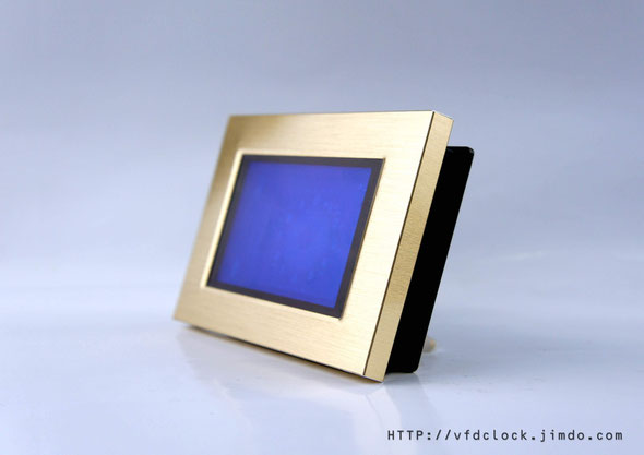
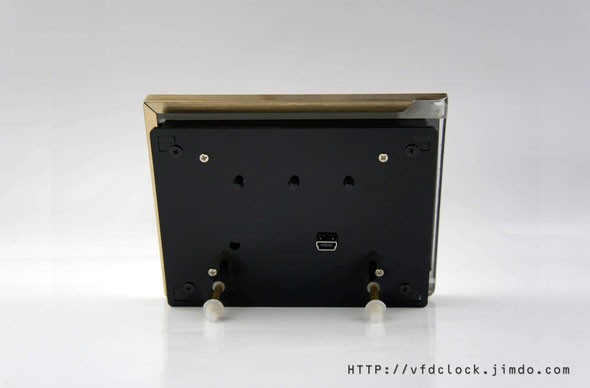
Comments: 8
-
#1
漂亮~
-
#2
My clock order has arrived today. The craftmanship is so good that my wife thought it was factory made. The use of the filter is a good design, by which the clock displays a beautiful sky blue colour. The selectable minute-hand movements are also interesting. Thanks Mr. Zhang for sharing your clock project!
-
#3
Hi. I would like to buy this for my daughter. What is the cost?
-
#4
To Lukasz Maciag:
please leave your email address,or search "VFD round clock" via EBAY.
Best regards. -
#5
Is your VFD Clock available in kit form?
-
#6
Now we have no kit for this item.
-
#7
Just got mine. Beautiful workmanship! My wife will love it!
-
#8
What is the cost? including economical shipping cost to Mexico City?
Sun
20
Jul
2014
Very Rare NEC CD66-A Single Digit NIXIE Clock V1.0-


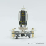
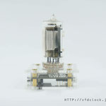

Very Rare NEC CD66A Single Digit NIXIE Clock V1.0
The NEC 66A NIXIE tube pics shown below are from:
http://www.ne.jp/asahi/shared/o-family/ElecRoom/PARTS/DISPLAY/ElCD66.html
ニキシー管 CD66 (NEC)


Sat
19
Jul
2014
USB供电的单管6E2猫眼音量指示器-USB Powered 6E2(EM84) Magic Eye VU Meter(Audio Visualizer)-V1.0
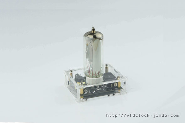
USB Powered 6E2(EM84) Magic Eye VU Meter(Audio Visualizer)-V1.0
Brand new,I designed and made it by myself.
Specifications:
Tube Name: 6E2(EM84) (BEIJING/SHANGHAI/SHUGUANG,Made in the P.R.C.);
Power Supply: 5V DC via MINI-USB;
Working Current: 500mA;
Size:58mm(L)*50mm(W)*80mm(H) ( with the tube installed);
PCB Size:48mm(L)*40mm(W);
PCB Color: Black;
Weight:50g(with the tube);
The 6E2 VU-meter works with any standard USB power supply,use only high-quality adapter!
Caution: High Voltage inside! For indoor use only!
Features:
1).5V Mini-USB powered,easy to be used.Small size&high efficiency.Can connect to your computer's USB plugs directly.
2).Round trimmer resistor installed on the right side of the case,easy for adjusting the circuit's sensitivity;
3).Tri-colored RGB LED mounted under the 6E2 tube. This LED can display any color with a lot of pre-defined colours as back light;
4).Simple setting by using 1 button only,can Turn ON&Turn Off the power and switch the LED's color or turn off the LED;
5).The tube is installed in the Ceramic Tube Socket or the Gold Plated Stamped Contacts.you can replace tube by yourself without using any tools;
6).Support 3.5mm Line_in and MIC (optional) on board,and also has a 3.5mm Line_out socket installed,you can just connect the VU-meter to your computer's sound output or other sound source and connect your headphone to the VU-meter;
7).Beautiful CAD designed acrylic case made using a laser cutter makes the clock look beautiful. You can assamble/disassamble the case by using only 4 screws on the bottom of the case.The case also has 4 bumpers as feet on the bottom of the case in order to stop to prevent case's damage.
For more information visit:
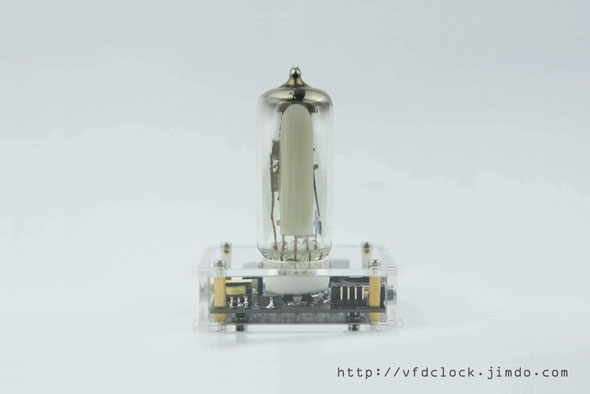
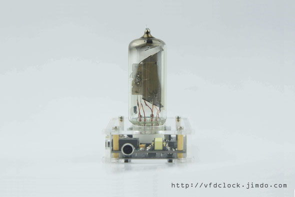
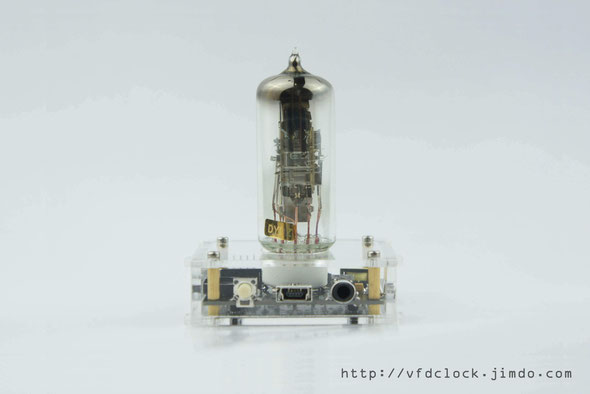
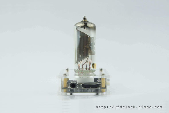

-
The circuit for driving 6E1 and 6E2 are the same,just need to change the few pins loc and some value of the resistor,we will create the 6E1 version next time,tks for your opinion.
-
#1
Good design!
Personally I like 6E1/EM80 more. I think it is more beautiful than 6E2. There is a web site : www.magiceyetubes.com which has a page to display almost(if not all) all magic eyes pattern. The 6E1 is readily available in Taobao and is not expensive. You may want to try it out!
Sat
19
Jul
2014
IN-8 and IN-8-2 Single Digit NIXIE Clock V1.0
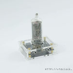

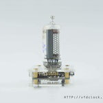


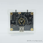
IN-8 Singled Digital NIXIE Clock V1.0
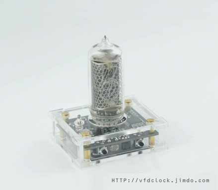
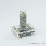

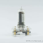
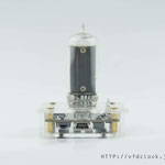

IN-8-2 Single Digital NIXIE Clock V1.0
Sun
15
Jun
2014
BOE圆盘荧光钟-USB Powered VFD48 Analog-style Unique Round VFD Clock
Old instructions
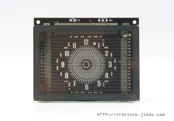
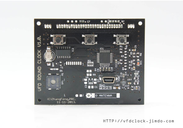
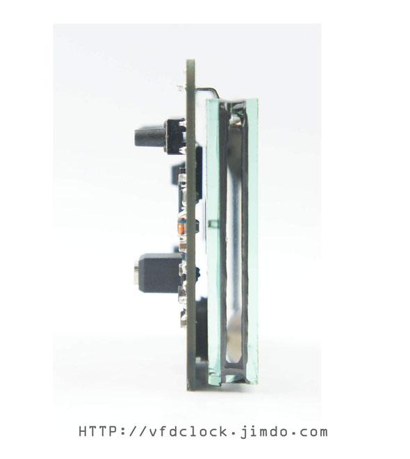
USB Powered VFD48 Analog-style Unique Round VFD Clock V1.0.-No enclosure
Specifications:
Panel Name: BOE VFD48 (Made in the P.R.C.);
Panel Size: :68mm(L)*48mm(W)*8.5mm(T);
Clock Supply: 5V DC via MINI-USB;
Working Current: <450mA;
Clock Size:70mm(L)*55mm(W)*15mm(H) ([*].20mm(H) with the button’s heads included)
PCB Size:70mm(W)*55mm(H);
PCB Color: Black or Blue;
Weight:61g;
The clock works with any standard USB power supply,use only high-quality adapter!
Caution: For indoor use only!
Features:
1).5V Mini-USB powered,easy to be used.Very slim design, no transformer ,high efficiency. Can connect to your computer's USB plugs directly.
2).Support displaying Year+Month+Day info on panel.
3).Support 2 different Effs:Normal/Quartz for displaying time.
4).High accuracy RTC inside,+-13 secons per month.
5).Simple setting by using 3 buttons only and support IR remote control(optional).
6).Three alarms with weekends ON/OFF support,can be controlled individually.
7).Three programmable Auto Power ON/OFF mode,can turn ON/OFF Clock in any time you want.This function can save VFD panel’s life.
8).8-level adjustable VFD brightness with Auto-brightness feature(optional,its ability to adjust the tube brightness depending on the current environment).
9).Rechargeable Backup Battery or Farad capacitor keeps RTC runing during power outages.
10).Store user settings in non-volatile memory.
For video(s):
http://youtu.be/mXAnQ2UBZp8
For more information visit:
http://vfdclock.jimdo.com
USB供电的VFD荧光圆盘指针时钟 V1.0.
规格Specifications:
面板名称Panel Name: BOE VFD48 (Made in the P.R.C.);
面板尺寸Panel Size: :68mm(L)*48mm(W)*8.5mm(T);
供电Clock Supply: 5V DC via MINI-USB;
工作电流Working Current: <450mA;
时钟尺寸Clock Size:70mm(L)*55mm(W)*15mm(H) ([*].20mm(H) with the button’s heads included)
印刷电路板尺寸PCB Size:70mm(W)*55mm(H);
印刷电路板颜色PCB Color: Black or Blue;
重量Weight:61g;
本时钟可使用标准USB电源适配器供电,请一定使用优质电源适配器!
The clock works with any standard USB power supply,use only high-quality adapter!
备注:仅供室内使用!
Caution: For indoor use only!
功能特性Features:
1).5V Mini-USB电源供电,高效超薄电路板设计,可直连电脑USB口使用;
2).支持年-月-日信息的显示;
3).支持二种时间显示方式:普通显示/仿石英钟显示;
4).高精度时钟,每月最大误差在±13秒以内;
5).本机可通过三按键操作,同时支持红外遥控器功能(可选功能);
6).提供三组独立的闹铃设置,支持周末闹铃关闭功能;
7).提供三组独立的自动开关机设置,此功能可提高VFD面板的使用时间;
8).8级可调的整体亮度设置,同时支持自动环境光检测功能(可选功能);
9).内置可充电电池或法拉电容作为RTC后备供电,可确保断电走时;
10).用户的设置被保存在内部EEPROM内,断电后无需重新设置;
Comments: 6
-
#1
这钟要是配一很cool的外壳就perfect!
-
#2
The case will coming soon!
-
#3
Regards
what is the cost? including economical shipping to Mexico City? -
#4
Hello, is this available in kit form to solder myself? Thank you!
-
#5
I also have the same question, Is if this is available in kit form for solder itself?
And I thank you for the opportunity to comment on your article, of course, I waited for the answer. -
#6
All the friends:
We have the KIT and fully assembled versions which you can find via my Ebay store.
http://stores.ebay.com/Nixie-Gadgets
Best regards.
Sat
10
May
2014
IN-14单管辉光时钟-1.1版-USB Powered IN-14 Single Digit NIXIE Clock V.1.1.
USB Powered IN-14 Single Digit NIXIE Clock V1.1
Now,It's capable of standing by itself with a Lithium-ion battery installed in it.(Battery Charge Function also included).
For more info:
http://vfdclock.jimdo.com
http://youtu.be/etFFZQKwRUg
http://v.youku.com/v_show/id_XNzEwMTIyMDYw.html
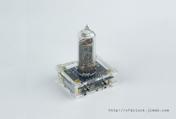
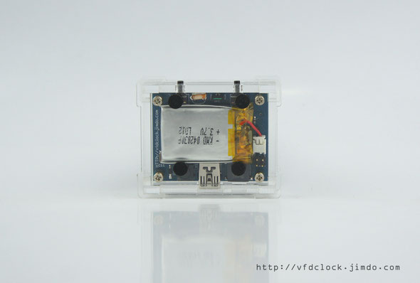

NEW-USB Powered IN-14 Single Digit NIXIE Tube Clock V1.1.
IN-14 Single Digit NIXIE Clock with acrylic enclosure
Brand new,I designed and made it by myself.
Notice:
In order to drive the NIXIE tube, some
internal equipments are under the High Voltage(up to 180V DC),please do not use this clock outside or in any wet conditions,please do not touch any part inside the clock when power supply is
turned on.Always keep it away from kids.
Specifications:
Tube Name:IN-14(Made in USSR)
Tube Diameter:18mm;
Tube Height:55mm(approx including glass nipple);
Digit Height,:17mm;
Digit Width:10mm;
Clock Supply: 5V DC via MINI-USB;
Max Current: <=250mA;
Clock Size:50mm(L)*42mm(W)*70mm(H)
PCB Size:40mm*32mm;
PCB Color:Blue/Black;
Weight:34g;(No including battery)
The clock works with any standard USB power supply,use only high-quality adapter!
Features:
1).5V Mini-USB powered,easy to be used. Can connect to your computer's USB plugs
directly.
2).Support 12H or 24H display modes, can show "."as“A/P" in 12H time
format.Leading zero blanking is programmable.
3).Display date in all format: YY.MM.DD or DD.MM.YY or MM.DD.YY or even MM.YY.DD.
4).Support 3 different Effs:Normal/Fading/Cross Fading/Slow Fading/Loop for displaying time.
5).High accuracy RTC inside,precision gap per month:13 secons.
6).Simple setting by using 2 buttons only and supports IR remote control(optional).
7).Three alarms with weekends ON/OFF support,can be controlled individually.
8).Three programmable Auto Power ON/OFF mode,can turn ON/OFF NIXIE tubes in any time you want.This function can save tubes life.
9).8-level adjustable NIXIE tube bright with Auto-brightness feature(its ability to
adjust the tube brightness depending on the current environment).
10).Rechargeable Backup Battery or Faradcapacitorkeeps
RTC runing during power outages.
11).Tri-colored RGB LED mounted under the NIXIE tube. This LED can display any color with a lot of pre-defined auto colour change
effects.
12).Store user settings in non-volatile memory.
13).Beautiful CAD designed acrylic case made using a laser cutter makes the clock look beautiful. You can assamble/disassamble the case by
using only 4 screws on the bottom of the case.The case also has 4 bumpers as feet on the bottom of the case in order to stop to prevent
case's damage.
14).Can install a Lithium-ion Battery as the internal power supply,with charger circuit (optional).
For video(s):
http://youtu.be/etFFZQKwRUg
For more information visit:
http://vfdclock.jimdo.com
Mon
05
May
2014
IN-18 Single Digit NIXIE Clock
USB Powered IN-18 Single Digit NIXIE Clock with acrylic enclosure V1.0.
IN-18 Single Digit NIXIE Clock with acrylic enclosure
Brand new,I designed and made it by myself.
Notice:
In order to drive the NIXIE tube, some
internal equipments are under the High Voltage(up to 180V DC),please do not use this clock outside or in any wet conditions,please do not touch any part inside the clock when power supply is
turned on.Always keep it away from kids.
Specifications:
Tube
Name: IN-18 (Made in the U.S.S.R.);
Tube Size:30mm(dia);
Tube Height:68mm(no including the legs and the glass
nipple);
Digit Height:40mm;
Digit Width:22mm;
Clock Supply: 5V DC via MINI-USB;
Working Current: <=350mA;
Clock Size:58mm(L)*54mm(W)*85mm(H)
PCB Size:48mm*44mm;
PCB Color: Blue or Black;
Weight:62g(weight with the tube installed);
The clock works with any standard USB power supply,use only high-quality adapter!
Features:
You can replace the tube by yourself without using any tools.
1).5V Mini-USB powered,easy to be used. Can connect to your computer's USB plugs directly.
2).Support 12H or 24H display modes, can show "."as“A/P" in 12H time
format.Leading zero blanking is programmable.
3).Display date in all format: YY.MM.DD or DD.MM.YY or MM.DD.YY or even MM.YY.DD.
4).Support 3 different Effs:Normal/Fading/Cross Fading for displaying time.
5).High accuracy RTC inside,+-13 secons per month.
6).Simple setting by using 2 buttons only and supports IR remote control(optional).
7).Three alarms with weekends ON/OFF support,can be controlled individually.
8).Three programmable Auto Power ON/OFF mode,can turn ON/OFF NIXIE tubes in any time you want.This function can save tubes life.
9).8-level adjustable NIXIE tube bright with Auto-brightness feature(its ability to
adjust the tube brightness depending on the current environment).
10).Rechargeable Backup Battery or Faradcapacitorkeeps RTC runing during power outages.
11).Tri-colored RGB LED mounted under the NIXIE tube. This LED can display any color with a lot of pre-defined auto colour change
effects.
12).Store user settings in non-volatile memory.
13).Beautiful CAD designed acrylic case made using a laser cutter makes the clock look beautiful. You can assamble/disassamble the case by
using only 4 screws on the bottom of the case.The case also has 4 bumpers as feet on the bottom of the case in order to stop to prevent
case's damage.
14).Support DS18B20 temperature sensor(optional).
For video(s):
http://youtu.be/TX9FV14szwM
For more information visit:
vfdclock.jimdo.com
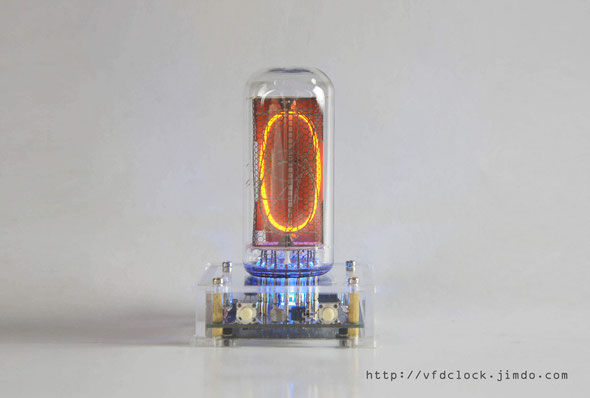
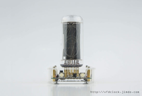
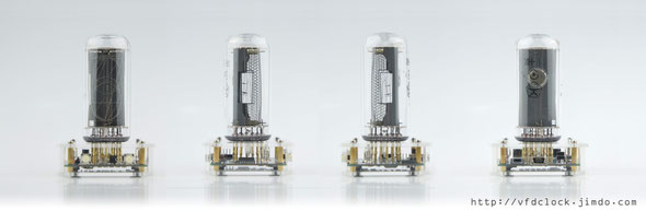
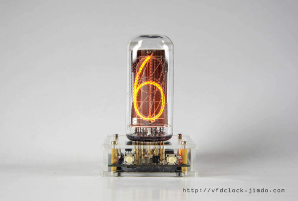

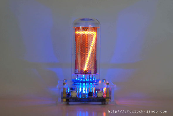
Mon
05
May
2014
QS27-1 单管辉光时钟 V1.0 QS27-1 Single Digit NIXIE Clock
USB Powered QS27-1 Single Digit NIXIE Clock with acrylic enclosure V1.0.
QS27-1 Single Digit NIXIE Clock with acrylic enclosure
Brand new,I designed and made it by myself.
Notice:
In order to drive the NIXIE tube, some
internal equipments are under the High Voltage(up to 180V DC),please do not use this clock outside or in any wet conditions,please do not touch any part inside the clock when power supply is
turned on.Always keep it away from kids.
Specifications:
Tube
Name: QS27-1 (FENGGUANG,Made in the P.R.C.)
Tube Size:27mm*20mm;
Tube Height:23mm(no including the legs and the glass nipple);
Digit Height:15mm;
Digit Width:10mm;
Clock Supply: 5V DC via MINI-USB;
Working Current: <=250mA;
Clock Size:52mm(L)*44mm(W)*45mm(H)
PCB Size:42mm*36mm;
PCB Color: Blue or Black;
Weight:42g(with the tilt-back legs installed);
The clock works with any standard USB power supply,use only high-quality adapter!
Features:
This clock can be placed horizontally,vertically and tilted with tilt-back legs installed.
You can replace the tube by yourself without using any tools.
1).5V Mini-USB powered,easy to be used. Can connect to your computer's USB plugs directly.
2).Support 12H or 24H display modes, can show "."as“A/P" in 12H time
format.Leading zero blanking is programmable.
3).Display date in all format: YY.MM.DD or DD.MM.YY or MM.DD.YY or even MM.YY.DD.
4).Support 3 different Effs:Normal/Fading/Cross Fading for displaying time.
5).High accuracy RTC inside,+-13 secons per month.
6).Simple setting by using 2 buttons only and supports IR remote control(optional).
7).Three alarms with weekends ON/OFF support,can be controlled individually.
8).Three programmable Auto Power ON/OFF mode,can turn ON/OFF NIXIE tubes in any time you want.This function can save tubes life.
9).8-level adjustable NIXIE tube bright with Auto-brightness feature(its ability to
adjust the tube brightness depending on the current environment).
10).Rechargeable Backup Battery or Faradcapacitorkeeps RTC runing during power outages.
11).Tri-colored RGB LED mounted under the NIXIE tube. This LED can display any color with a lot of pre-defined auto colour change
effects.
12).Store user settings in non-volatile memory.
13).Beautiful CAD designed acrylic case made using a laser cutter makes the clock look beautiful. You can assamble/disassamble the case by
using only 4 screws on the bottom of the case.The case also has 4 bumpers as feet on the bottom of the case in order to stop to prevent
case's damage.
For video(s):
youtu.be/hqaDd8wrhFg
For more information visit:
vfdclock.jimdo.com

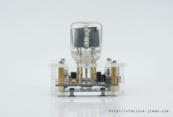

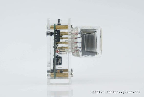

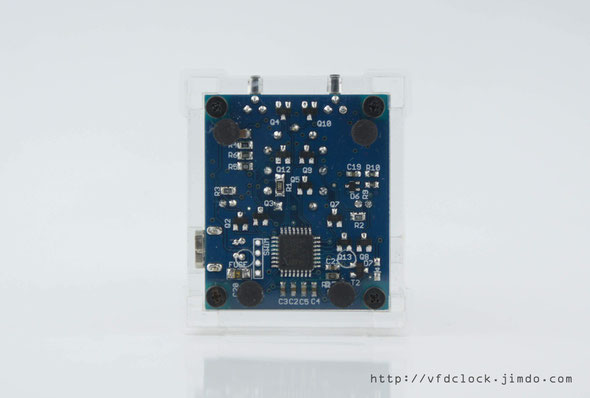
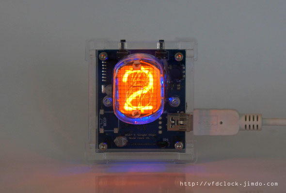
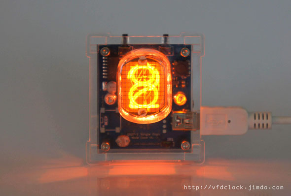
Wed
02
Apr
2014
IV-11 单管VFD时钟 IV-11 Single Digit VFD CLock V1.0
IV-11 Single Digital VFD Clock V1.0


Wed
02
Apr
2014
IN-12A/B 单管辉光时钟,IN-12A/B Single Digit NIXIE Clock V1.0
IN-12A/B Single Digital NIXIE Clock V1.0
Specifications:
Tube Name: IN-12A/B (Made in the U.S.S.R.)
Tube Size:30mm*20mm;
Tube Height:26mm(no including the legs and the glass nipple);
Digit Height:17mm;
Digit Width:10mm;
Clock Supply: 5V DC via MINI-USB;
Working Current: <=250mA;
Clock Size:52mm(L)*44mm(W)*45mm(H)
PCB Size:42mm*36mm;
PCB Color:Black;
Weight:43g(with the tilt-back legs);
The clock works with any standard USB supply,use only high-quality adapter!
Features:
This clock can be placed horizontally,vertically and tilted with tilt-back legs installed.
You can replace the tube by yourself without using any tools.
1).5V Mini-USB powered,easy to be used.Can connect to your computer's USB plugs directly.
2).Support 12H or 24H display modes, can show "."as“A/P" in 12H time format.Leading zero blanking is programmable.
3).Display date in all format: YY.MM.DD or DD.MM.YY or MM.DD.YY or even MM.YY.DD.
4).Support 3 different Effs:Normal/Fading/Cross Fading for displaying time.
5).High accuracy RTC inside,precision gap per month:13secons.
6).Simple setting by using 2 buttons only and supports IR remote control.
7).Three alarms with weekends ON/OFF support,can be controlled individually.
8).Three programmable Auto Power ON/OFF mode,can turn ON/OFF NIXIE tubes in any time you want.This function can save tubes life.
9).8-level adjustable NIXIE tube bright with Auto-brightness feature(its ability to adjust the tube brightness depending on the current environment).
10). Rechargeable Backup Battery or Farad capacitor keeps RTC runing during power outages.
11).Tri-colored RGB LED mounted under the NIXIE tube. This LED can display any color with a lot of pre-defined auto colour change effects.
12).Store user settings in non-volatile memory.
13).Beautiful CAD designed acrylic case made using a laser cutter makes the clock look beautiful. You can assamble/disassamble the case by using only 4 screws on the bottom of the case.The case also has 4 bumpers as feet on the bottom of the case in order to stop to prevent case's damage.
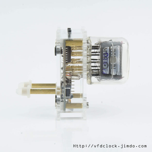


Wed
05
Mar
2014
为ARDUINO设计的QS30-1辉光管模块 QS30-1 NIXIE tube module for ARDUINO v1.0
AA battery driveable QS30-1 NIXIE Module for Arduino / AVR / PIC / STM / ARM /PI V1.0.
Notice:
In order to drive the NIXIE module, some internal equipments are under the High Voltage(up to 180V DC),please do not use this module outside or in any wet conditions,please do not touch any part inside the module when power supply is turned on.Always keep it away from kids.
Specifications:
Tube Name:QS30-1(FENGGUANG);
Module Supply: 2V~7V DC;
Max Current: <=150mA;
Module Size:38mm(L)*38mm(W)*43mm(H);
PCB Size:38mm*38mm;
PCB Color:Black;
Weight:38g;
The module works with 2 AA batteries (in serial),and also works with any standard USB power supply,use only high-quality adapter!
Features:
1).Very small size module,only 38mm*38mm,fits for a lot of tiny EE works;
2).Wild supply range,works fine with any 5V USB powered ARDUINO or other 5V/3V3 MCUs ,easy to be used. For driving less than 5 modules together,can connect to your computer's USB plugs directly.(For working under 3V,the Blue/Green LED may not be able to light up,but the NIXIE tube and red led work fine).
3).High effenciency design,low current.Usually one module needs only about 100mA current under 5V DC supply,so for 1~8 modules can be drived together via regular Dupont Line.For driving over 4 modules together,recommand you using a 5V/1A USB adapter.
4).Module contains a self testing switch,when press the test key down,the NUM-"8" will light up,easy for tesing the module.
5).74HC595 driving chips,simple 3-wire SPI interface,with /OE and HVEN pins,can adjust the global brightness via PWM signal and shutdown the High Voltage completely.
6).Contains over-current protection, and reverse connection protection circuits.
7).With 2 dots on the right and left side,you can create not only the NIXIE clock app but also the "Divergence Meter" from the Steins' Gate style looking with 8 modules.
8).Open source ARDUINO NUO source code,provide high level nixie_printf() function,easy to be used,can control the left and right dots in this function either.
9).We provide extra 1PCS acrylic back board for connecting 2,4,6,8,10 modules together for free.
10).Tri-colored RGB LED mounted under the NIXIE tube.
11).Beautiful CAD designed acrylic casemade using a laser cutter makes the module look beautiful. You can assamble/disassamble the case by using only 4 screws on the bottom/top of the case.
Interface:
3-wire SPI for 74HC595
+5V
GND
DAT
CLK
LATCH
/OE - ouput enable(optional)
HVEN - High voltage enable(optional)
Video(s):
http://youtu.be/dlNi5vbduUY
http://youtu.be/aVq1RkWnuYs
http://youtu.be/y0Ldc_qxzdU
For more information visit:
http://vfdclock.jimdo.com


简单介绍一下尺寸与功能:
1、外观尺寸为38mm(L)*38mm(W)*40mm(H);
2、供电规格:2V~7V全兼容,推荐5V工作;单模块消耗电流约100mA(5V)。在3V以下供电时,LED中的蓝色与绿色无法点亮,但是红色LED与辉光管工作正常;
3、简单的双74HC595驱动方案,总共7根外接线,分别是:
+5V 电源
GND 地
DAT 数据
CLK 时钟
LATCH 锁存
/OE 输出有效
HVEN 高压有效
最小只需要三根IO线即可驱动(DAT,CLK,LATCH),/OE与HVEN可以忽略不接。也可以通过PWM信号控制/OE线来控制整体亮度,HVEN线则可以完全控制开启/关闭高压部分;
普通ARDUINO UNO即可控制,通常一个PC提供的单USB口可提供5V 500mA供电,使用普通杜邦线即可直接控制4只显示模块串联工作。经过2星期的程序测试,在LED全显示,NIXIE管道最高亮度情况下,4联模块程序工作,完全没有任何问题,除LED与显示管外,无任何零件有发热现象。
(图片内的四联板即为使用普通ARDUINO UNO直连电脑驱动的)
4.全部QS30-1显示管使用的都是从上千只管中精选出来的最高质量的风光管,确保显示的完美,绝无笔画断开、显示不全、显示暗淡等现象(绝非通过后期高压大电流自行“修复”的低寿命管子),同时配合高效率的升压电路,从根本上确保了绝对完美的辉光显示效果;
5、提供2联、4联、6联、8联背板,可以固定连接不同数量需求的模块组,在整体模块数量超过6只但是不超过10只的情况下,可简单换用外部5V 1A的USB电源适配器供电即可正常工作,不需要使用特殊的供电设备;
6、所有模块全部自带过电保护及电源反接保护电路,反接与过流都不会烧坏电路;
7、除QS30-1外,还在管子的左右侧各增加了一个点号,总共提供12个显示段,不仅可以完成如时钟、数字等的显示模块功能,只要组合8个模块,也可以完成“命运石之门”(原名:Steins;Gate;日语:シュタインズ・ゲート)中的“世界线变动率探测仪(Divergence Meter)”显示效果,届时会免费提供对应的源程序;
8、提供完整的ARDUINO UNO驱动源程序,支持高级nixie_printf()函数,用户可直接使用与printf()函数相同的规格参数简单地完成显示操作,可直接在参数中控制左右的点号,无需使用另外的函数。例如下图中的循环数字显示效果的输出函数为:
for (i=0; i<=9999; i++)
{
nixie_printf("%02d.%02d", i/100, i%100);
delay(50);
}
即可循环显示从00.00到99.99
应用代码就是这么简单;


Sat
01
Mar
2014
QS30-1单管时钟-1.0版-QS30-1 Single Digit NIXIE Clock Ver.1.0.
TAOBAO网的购买地址为:
标准版:
http://item.taobao.com/item.htm?id=37549627997
增强版:
http://item.taobao.com/item.htm?id=37550399222
标准版不带CDS光感、不带LED、不带红外遥控功能,其他同增强版;
QS30-1 Single Digit NIXIE Clock with acrylic enclosure V1.0.
增强版-QS30-1 单管辉光管时钟 V1.0
QS30-1 Single Digit NIXIE Clock with acrylic enclosure;Brand new,I designed and made it by myself.
注意事项Notice:
辉光管为高压驱动设备,内部包含180V直流高压,请勿在室外或者潮湿的环境下使用,请勿让儿童接触使用;
In order to drive the NIXIE tube, some internal equipments are under the High Voltage(up to 180V DC),please do not use this clock outside or in any wet conditions,please do not touch any part inside the clock when power supply is turned on.Always keep it away from kids.
产品规格Specifications:
显示管名Tube Name:QS30-1(国产优质风光管)
电源Clock Supply: 5V DC via MINI-USB;
最大工作电流Max Current: <=250mA;
产品尺寸Clock Size:52mm(L)*52mm(W)*40mm(H)*不计斜撑支脚
印刷电路板尺寸PCB Size:42mm*42mm;
印刷电路板颜色PCB Color:黑色Black;
产品重量Weight:52g;
时钟可使用任何USB电源适配器驱动,请一定使用优质的电源适配器!
The clock works with any standard USB power supply,use only high-quality adapter!
功能特性Features:
本时钟提供三种摆放方式:水平放置、垂直放置,安装上背面支撑脚后也可以倾斜放置(推荐)。
1).5V Mini-USB 电源供电,可直接与USB口连接;
1).5V Mini-USB powered,easy to be used. Can connect to your computer's USB plugs directly.
2).支持12小时与24小时时制,支持以[.]号表示"AM/PM",支持开启或关闭前导零功能;
2).Support12Hor24Hdisplay modes, can show "."as“A/P" in 12H time format.Leading zeroblanking is programmable.
3).支持以所有可能的四种顺序显示日期;
3).Display date inall format: YY.MM.DD or DD.MM.YY or MM.DD.YY or even MM.YY.DD.
4).支持三种之间显示切换方式:普通切换/渐变切换/交叉渐变切换;
4).Support 3 different Effs:Normal/Fading/Cross Fadingfor displaying time.
5).高精度时钟,每月最大误差在+-13秒以内;
5).High accuracy RTC inside,precision gapper month:13 secons.
6).本机双按键操作,同时支持红外遥控器操作;
6).Simple setting by using2 buttonsonly andsupportsIR remote control.
7).提供三组独立的闹铃设置,支持周末闹铃关闭功能;
7).Three alarms with weekends ON/OFF support,can be controlled individually.
8).提供三组独立的自动开关机设置,此功能可提高NIXIE管的使用寿命;
8).Three programmable Auto Power ON/OFFmode,can turn ON/OFF NIXIE tubes in any time you want.This function can save tubes life.
9).8级可调的整体亮度设置,同时支持自动环境光检测功能;
9).8-level adjustable NIXIE tube brightwithAuto-brightnessfeature(its ability to adjust the tube brightness depending on the current environment).
10).内置可充电电池作为RTC后备供电,可确保长时间断电走时;
10).Rechargeable Backup Batterykeeps RTC runing during power outages for more than weeks when battery is fully charged.
11).管子下方的真彩色RGB LED可显示任意色彩,具备呼吸灯效果及多种内置的色彩切变效果;
11).Tri-colored RGB LEDmounted under the NIXIE tube. This LED can display any color with a lot of pre-defined auto colour change effects.
12).用户的设置被保存在内部EEPROM内,断电后无需重新设置;
12).Store user settings innon-volatile memory.
14).CAD设计及激光切割的全透明亚克力外壳,仅使用底部的四颗螺丝即可完成组装;外壳底部同时包含4只橡胶脚垫,确保摆放稳定,同时可防止刮花外壳或桌面;
14).Beautiful CAD designedacrylic casemade using a laser cutter makes the clock look beautiful. You can assamble/disassamble the case by using only 4 screws on the bottom of the
case.The case also has4 bumpersas feet on the bottom of the case in order to stop to prevent case's damage.


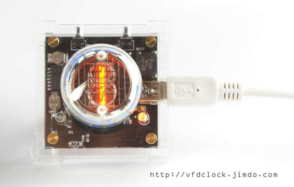

Thu
20
Feb
2014
IN-14单管时钟-1.0版-IN-14 Single Digit NIXIE Clock Ver.1.0.
TAOBAO网的购买地址为:
IN-14 单管辉光管时钟
版本:1.0. (02-18-2014).
相关产品及后续升级等信息,请访问:http://vfdclock.jimdo.com
或通过email与作者联系:zjjszhangf@gmail.com
注意事项:
辉光管为高压驱动设备,内部包含180V直流高压,切勿在室外或潮湿环境下使用,同时勿让儿童接触使用!
请勿将此产品用于商业、工业、医疗用途或其他可能对人身安全产生危害的特殊用途装置上。对此产品或设计所产生或引起的任何财产损失或法律纠纷,包括直接的与间接的,本人不承担任何责任。
产品规格:
显示管名称:IN-14(前苏联制造);
显示管直径:18mm;
显示管高度:55mm(包含顶部玻璃气嘴);
数字高度:17mm;
数字宽度:10mm;
电源:直流5V (MINI-USB);
最大工作电流: <=250mA;
产品尺寸:50mm(长)*42mm(宽)*70mm(高);
印刷电路板尺寸:40mm*32mm;
印刷电路板颜色:黑色;
产品重量:34g;
以上规格若有更改,恕不另行通知。
本时钟可使用普通USB电源适配器驱动,请一定选用优质的电源适配器!
功能特性:
1).5V Mini-USB电源供电;
2).支持12小时与24小时时制,支持以[.]号表示"AM/PM",支持开启或关闭前导零显示;
3).支持四种顺序显示日期:YY.MM.DD 或 DD.MM.YY 或 MM.DD.YY 或 MM.YY.DD;
4).支持三种时间显示切换方式:普通切换/渐变切换/交叉渐变切换;
5).高精度时钟,每月最大误差在±13秒以内;
6).本机可通过双按键操作,同时支持红外遥控器功能;
7).提供三组独立的闹铃设置,支持周末闹铃关闭功能;
8).提供三组独立的自动开关机设置,此功能可提高NIXIE管的使用时间;
9).8级可调的整体亮度设置,同时支持自动环境光检测功能;
10).内置可充电电池作为RTC后备供电,可确保长时间断电走时;
11).管子下方的真彩色RGB LED可显示任意色彩,具备呼吸灯效果及多种预置的色彩转变效果;
12).用户的设置被保存在内部EEPROM内,断电后无需重新设置;
13).可选DS18B20作为温度传感器(可选件,未包含在本产品内);
14).CAD设计、激光切割的全透明亚克力外壳,仅使用底部的四颗螺丝即可完成组装;外壳底部同时包含4只橡胶脚垫,确保摆放稳定,同时可防止刮花外壳或桌面;
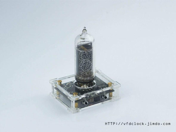

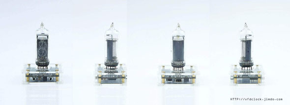
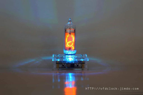

Wed
29
Jan
2014
为Arduino设计的全隔离QS30-1辉光放电数字管模块

本文为版权内容,文章内容(包括但不限于文字、图片、声音、录像、图表、软件、程序)未经版权人书面许可,任何人不得引用、复制、转载、摘编或以其他任何方式非法使用。
Copyright material!
All material on this page is copyright of ZhangFeng(zjjszhangf@gmail.com) unless otherwise acknowledged. Duplication or sale of all or any part of it is not permitted.
作者:张锋 (zjjszhangf@gmail.com)
功能特点
1、使用常见的QS30-1型NIXIE管,字符尺寸较大,显示效果好,且管子价格低廉,有配套管座,业余条件下采购容易;
2、NIXIE供电部分采用全隔离变压器设计,实现低压与高压之间的隔离;信号传输部分使用光电耦合器进行连接,使得内部驱动与外部信号线路完全电气隔离;隔离变压器与光耦双管齐下,可确保整体模块使用上的安全性,保护外部驱动电路及使用安全;
3、使用灰度动态驱动技术,使用专门定制程序的双单片机构成内外隔离的显示驱动电路与信号驱动电路,整体电路结构清晰,实现了低成本与小尺寸驱动;
4、模块默认引出标准的SPI数据通讯接口,即可以直接使用SPI口通讯,又可以模拟其他类型的接口电路,不仅支持ARDUINO平台驱动,也可以连接普通单片机,模块既可单独运作又可两两串联多个运作,只要确保数据可以在各独立模块之间传递即可;
5、主电源使用常见的单一+5V供电,无需更高的电压,对于1~2个模块组合工作的情况下,只要供应电流足够,可直接使用ARDUINO模块直接供电,而无需增加外部电源适配器,应用更加简捷;
6、NIXEI管下方选用RGB全彩LED作为底光显示器件,可实现任意灰度的真彩色显示切换,板上硬件自动实现灰度PWM效果,大大节约外部软件资源;配合ARDUINO应用软件,可实现呼吸灯等多种切换效果,整体显示效果绚丽多彩。
7、NIXIE显示模块自主支持16级灰度显示效果,不仅可以实现多种亮度调节,也可通过外部软件实现淡入淡出等多种NIXIE转场效果,显示效果优秀;
8、自带NIXIE修复功能,可实现开关切换输出电流,在修复模式下可为显示段提供2倍工作电流,可在一定程度上修复常见的显示笔段断开的问题;配合外部ARDUINO驱动,可实现更加复杂的自动定时修复功能,确保NIXIE管的正常显示;
QS30-1辉光管简介
QS30-1是我国上世纪生产的常见的NIXIE显示管,通称“辉光放电数字管”。其外观结构为圆形,端面显示(顶部显示)管,管脚位于管子底部,为直插粗管脚。此管主要设计用于计算机和数字仪器、仪表的数字显示用途。显示内容为数字0~9,10个数字分层排列,发光颜色为橙红色,晚间显示效果较好。
Nixie管的基本原理就是辉光放电,在管子内部充有稀薄的惰性气体,当管子两极的电压加大到一定值时,气体中的残余正离子被电场加速,获得足够大的动能去撞击阴极,产生二次电子,气体导电发光。所以在辉光管内部看不到类似VFD管那种由多种金属盐蒸发形成的银黑色吸气层,因为其内部本生就充有一定量的惰性气体。辉光放电管的主要特点就是放电区内光区有明暗层次,所需驱动电流小,基本不出现升温。缺点是需要较高的驱动电压,整体耗电较大,发光效率低。
从本质上讲辉光放电数字管与普通氖泡管的发光原理是一致的,但是区别在于辉光放电数字管引脚分正负极,而大部分非特殊结构的普通两脚氖泡既可以直流驱动,又可以交流驱动,是不分正负极的。产生这一区别的原因实际很简单,我们只需要做一个小试验即可了解:当我们给普通氖泡连接上直流启辉电压后(请选用透明的氖泡,便于观察),仔细观察氖泡内的两根电极,就会发现只有在负极端的金属电极周边有一团气体发光层,而在正极电极上则无发光层。辉光放电数字管正是利用了这一特点,将其中接负极的引脚弯成了数字的形状而已,而为了防止其他连接部位发光,在其外部增加了氧化物保护层。

QS30-1全管总计13只管脚,管脚直径约1.0mm~1.3mm,内部线路连接简单,Pin1与Pin8引脚为空脚,Pin2脚为阳极,其余10引脚则为数字0~9对应的阴极。详细参数如下。
|
引脚号 |
1 |
2 |
3 |
4 |
5 |
6 |
7 |
8 |
9 |
10 |
11 |
12 |
13 |
|
功能 |
空脚 |
阳极 |
阴0 |
阴9 |
阴8 |
阴7 |
阴6 |
空脚 |
阴5 |
阴4 |
阴3 |
阴2 |
阴1 |
QS30-1简单电气参数如下:起辉电压150V,熄灭电压100V,正常工作时阳极电压直流170V,消耗电流1.5~3.0mA(典型值为2.25mA)。更加详细的参数请参考《中华人民共和国第四机械部标准QS30-1辉光放电数字管 SJ1123-76》或管盒内所附带的说明书。
从引脚结构上来看,由于QS30-1使用的是硬管脚,所以在安装方法上可以采取直焊方式或者管座焊接方式进行,一般推荐使用管座安装,主要是考虑到日后更换方便,毕竟拆焊一个13脚的硬引脚连接不仅麻烦而且容易破坏PCB焊盘,得不偿失。
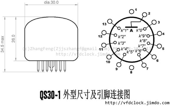
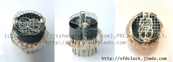
QS30-1辉光管实际特性
从实际采购与测试的情况来看,国内的QS30-1型号的NIXIE管主要有一下品牌,上海风光的QS30-1、上海产的SZ-3型(管脚与外观与QS30-1一致,仅标号不同),南昌牌QS30-1与宇宙牌的QS30-1。
对市场上这些不同品牌、不同型号、不同生产年份的QS30-1及其兼容管的测试情况来看,上海风光的QS30-1与SZ-3的做工与质量最好,只要管子前网没有明显发黑、没有漏气,在标准工作电压下,大部分都可正常工作,显示亮度也佳,大部分字符都可以正常显示,仅小部分显示不全。从结构上看,这些管子在尺寸与外观上基本一致,仅在内部面网结构上有差别,其中上海产的管子大部分是方格型亮银色网,显示效果最好,另外一些是蜂窝状的黑色面网,显示效果较差。
这些管子由于生产年限久远加上当年生产技术的关系,完美程度不高,常见的一个通病就是显示笔段不完全,尤其是在标准供电电压下,很多的南昌牌与宇宙牌的管子显示亮度很差,很多笔画多处显示不全,这个问题在最初开发的时候搞的非常头痛。后来经过实际测试,找到的解决方法也比较简单,那就是提高驱动电压与降低限流电阻。通过实际的测试发现,只要不是老化非常严重的管子,一般驱动电压提高到200~250V左右,限流电阻阻值降低20%~30%左右时,大部分的管子都可以确保正常的显示亮度。极个别的管子如果依旧有个别的字符显示不全,则可尝试进行活化修复处理。
所以根据以上的情况,基本确定本制作的基础驱动高压为高于200V直流驱动电压。
辉光管常用驱动方法
辉光管在电气驱动上的主要特点就是需要一个低电流的直流高压,所以整个控制电路的设置关键就转变成如何生成高压及控制直流高压的通断,以下就针对这两个基本应用需求进行方案设计。
先来看一下直流高压的控制方法:通常由低电压信号(常见的由单片机I/O口输出或者由低压逻辑电路输出的控制信号)控制高压信号的方法主要是几种:首先是控制元件的选型,可以使用4017等常规高压IC或者使用如Supetex HV系列高压串转并IC,常见的HV513或HV514都可以控制输出+250V的电压,完全满足NIXIE驱动的需要。但是缺点也很明显,就是HV513或HV514价格很高,极大地增加了制作成本。所以控制零件应该考虑使用分立元件以降低成本。
如果选择分立元件驱动,典型的控制高压用的分立元件可选继电器、可控硅、高压光电耦合器、高压三极管、高压MOSFET等,以本制作的小电流特点来看,选择高压三极管或者高压MOSFET进行控制是比较合适的,实际选择的是高压三极管,一来小尺寸封装的高压三极管很容易购买到,二来高压三极管的价格也很低,从成本上考虑,选择三极管进行控制比较合适。
使用三极管的当开关控制高电压的驱动方式有两类,一类是使用NPN型三极管控制对地端的通短,这种情况下一路驱动只需要一只三极管即可实现;另外一类是使用NPN+PNP组成电平移位电路对高压的高端进行开关控制,优点是可对阳极进行控制,可应用在多阳极的辉光管驱动电路或者动态扫描驱动电路中。这里的QS30-1是单一阳极的NIXIE管,可以使用NPN三极管组成控制对地导通的电路。
驱动三极管需要增加现流电阻,通常有两种选择,一是通用的在每个三极管的基极增加限流电阻,控制三极管的开关状态,优点是通用,可同时开关任何的三极管,缺点是所需的限流电阻数量多;另外一个方案是考虑到NIXIE驱动的特殊性,通常情况下在同一个时间段内一般只有一个显示字符被点亮,则可以考虑将所有驱动三极管的发射极连接在一起,统一使用一个限流电阻接地。这一电路的优点是只需要一只限流电阻,缺点是开关电流浪费较多,而且多三极管同时开启时,工作状态不稳定;

综合以上驱动方式,最后确定选择三极管限流部分采用在基极增加电阻的方案,确保输出的稳定性质与减少驱动电流。由于至少需要驱动12个输出端,考虑到焊接的复杂性及减少PCB面积的需求,限流电阻可以选择0603的排阻,以降低成本与减少元件尺寸。
考虑到QS30-1辉光管的结构比较简单,内部连接也不复杂,而且本制作采用的是静态连接,对阳极不需要进行控制,所以驱动电路选择的是使用NPN型三极管进行对地开关控制,0~9数字的每个阴极都对应设置一个NPN三极管作为开关,在三极管控制端的限流电阻的设置上,通常每段独立控制的电路都将限流电阻设置在三极管的基极,以独立控制每一路的开关电流。另外一种方案则适合在应用中不出现所有显示段都全部点亮的情况下使用,通常情况下大部分NIXIE同一时间只有一个字符段点亮(在动态显示切换过程中可短时出现2个左右的字符同时点亮的情况),所以整体所需控制的电流值很小,只有几mA,此时可将限流电阻移动到三极管的发射极,所有阴极控制三极管共用一个限流电阻,以减少电阻数量与布线上的复杂度。限流电阻的典型选值范围为10kΩ~33kΩ左右,具体值根据所选三极管的饱和放大值进行计算或者通过试验确定。
高压的生成及安全防护问题
由于本制作是作为一个由外部供电且具备外接通讯引脚的模块,内部包含有>170V的高压,已经大大超过了安全电压范围,所以在电路设计中需要考虑到高压防护的问题。
生成高压存在的以下一些难点,首先是如何升压的问题。考虑到制作尺寸的限制,升压方案的基本要求就是效率高、尺寸小、成本低、安全性好。要做到以上的要求,第一个想到的升压方案就是使用传统的BOOST电感升压电路来完成,但是由于需要输出200V以上的高电压,传统的BOOST专用芯片内的MOS管均无法达到200V的耐压要求,所以需要选择可带外扩MOS管的BOOST芯片配合外部高压MOSFET进行高压升压。另外一个问题是如果输入的供电电压是5V,由于PWM 占空比例的限制,需要控制95%甚至以上的占空比,增加了电路实际控制上的难度;同时,在驱动管的选型上,如果仅选择使用微型封装的普通高压三极管,工作频率将受到很大的限制,导致只能使用容量较高的输出电容,不仅成本高,而且高压高容电容尺寸大,蓄能多,安全性上也无法保障。另外一种方案是选择使用高压MOSFET管驱动,虽然高压MOSFET在频率相应、高压耐压与输出功率上都能够满足应用要求,但是如SOT-23这样小尺寸封装的高压MOSFET管很少,通常市场上只能买到基本都是大功率管,封装尺寸比较大,不利于本制作的小型化。而且大部分的高压MOSFET管通常都需要9V或者以上的门驱动电压,部分管子在5V驱动电压下仅能够做到勉强导通甚至可能根本无法导通,导致电路不工作或效率低下。如果增加辅助升压电路又导致零件增多,线路复杂化,得不偿失。
解决DC/DC升压比的问题的一种方案是参考微型闪光灯电路,使用专用的微型闪光灯变压器。通常这样的变压器都是专业工厂制造的,具备1:10~1:12的线圈比例,可以很轻松地从5V电压升到300V左右的高压,通常这类变压器是为了从3V电池供电转换到320V左右的输出高压定制的专用型变压器。它的优点的质量好,尺寸小巧,且最高可输出5mA左右的电流,非常适合驱动单一的NIXIE管。升压驱动也非常简单,使用典型的FlyBack反激变压器驱动电路即可。在实际制作过程中,专门购买了专用的驱动芯片与微型变压器进行测试电路的制作,最后的结果是输出电压很容易就可以达到200V,连接适当的限流动电阻后,完全可以驱动QS30-1型的NIXIE管。
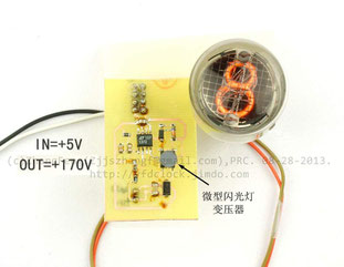
以上电路的优点是尺寸小,线路简单,虽然效率稍低,但是零件用的很少,很容易制作与调试。
实际上,上面这一电路在试制过程中,经实际实验,虽然电路的生成的200V电压很高,但是由于变压器尺寸的限制,实际输出电流极小,实测工作电流只有1.5mA~3mA左右(极限电流<5mA),同时由于使用了高频驱动方案,所安装的高压电容的容量也很小,只有0.47uF~1uF,这样的电路能够提供的实际输出能量是极低的,通过实际单手指触摸测试(请勿模仿),虽然只有瞬间极轻微电麻感,但是依旧不建议用户在使用过程中接触到模块内部任何的高压电路部分。如果要使用这一类型的电路,应该在电路PCB上印刷警告信息同时利用外部的亚克力外壳来防护,以防止手指接触到内部的电路。
首套设计方案
在正式进入本设计的详细说明前,先提一下先前所使用的首套套制作方案,这一制作方案是使用非常规驱动模式配合高压变压器完成的驱动模块。
实际上,除了上文中所述的几种驱动方案外,驱动NIXIE还有另外一种非常规的驱动方式,那就是利用NIXIE的起辉与熄灭之间大约50V的电压差以及利用NIXIE本身的稳压特性,利用稳压管,配合中耐压的开关电路,对NIXIE的阴极进行控制。通常如HV5812中压驱动芯片可输出+80V的电压,当其输出为0时,输出拉地,电压满足点亮要求,NIXIE对应的笔画点亮,当输出为高时,对地电压被抬高,NIXIE阳极与地之间的电压差不足以点亮NIXIE管,则对应的笔画熄灭。这种非常规的驱动方法的优势在于可以使用价格低廉的中耐压驱动芯片驱动高电压的NIXIE的亮灭,
这一方案的特点是所需零件少,可以使用以前开发的VFD驱动底板作为驱动板,仅需要再设计一片新的上板即可工作,所需投入较小,而且相关驱动软件也仅需在原驱动VFD软件的基础上稍做修改就可以。
在实际测试电路的制作过程中,专门使用了此电路制作了与先前发表的《ARDUINO通用荧光数码管模块》底板配套的NIXIE上板,在测试电路中使用了微型变压器生成高压的方法以减少体积,如图可见所有零件全部可以塞在QS30-1插座的管脚内圈的范围内,直接利用下板的中压升压芯片来完成NIXIE的开关控制,实际测试的结果确定这个方案是可行的,但是实际应用中,这个方案存在一些实际问题。
首先是安全方面的问题,由于电路使用非隔离高压升压方案,而且驱动电路使用耐压不足中压驱动芯片,再加上没有设计特别的保护措施,虽然在正常情况下电路工作正常,但是一旦出现例如用户插入了一只存在阴极短路的NIXIE管,则会导致高压直接灌入这些芯片,会造成驱动芯片损坏,严重的情况下还可能损坏用户连接在电路中的其他设备。
其次是经过实际测试,虽然输出的电压可以达到170V的QS30-1管的起辉电压,但是由于大部分管子年代都比较久远,很多管子在这样的标准起辉电压中都无法实现完全点亮笔段,实际显示效果并不完美。当然,如果换用一些前苏联或者德国生产的NIXIE替换管,虽然大部分管子的显示都没有问题,但是这些进口的管子价格比较高,会极大地增大生产成本,全部换成进口管不太现实。
由于以上设计存在着高压应用上的安全问题,虽然使用了微型变压器来解决升压比的问题,但是实际使用的依旧是非隔离升压方案,所以整个电路生成的高压依旧是与外部电源共地的,依旧存在安全问题。所以在使用这一设计时建议使用独立的电源适配器或者使用隔离变压器,并使用光耦进行通讯隔离方可确保使用安全。
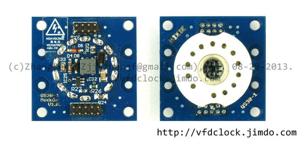

高压隔离的考虑
实际上包含高压输出的模块,应该重点考虑电气安全问题,由于电路使用的是简单无隔离的共地高压电路,在日常使用中很可能因为电路板受潮、污染等原因引起高压串入外部电路,极可能导致外部驱动电路损坏。用户驱动模块大都使用单片机系统,而大部分单片机系统都是通过烧写器等设备连接电脑的。高压可能意外通过线路串入外部设备,有可能造成用户的外部系统甚至电脑损坏,而且大部分开发板很多都是裸板,各种接点裸露,高压串出也极容易造成触电危险。所以在这个问题的处理上,本制作最后确定一定要增加电源隔离与信号隔离的措施,以确保安全性。
电源隔离方案可选择的余地不多,使用的也是基本的变压器,最简单的就是所有模块不使用电源隔离,而是在与外部电路的连接中统一使用一个独立的电源与信号隔离模块,电源隔离模块可以使用高频变压器制作,以减小体积,信号隔离模块可选择使用光电耦合器来制作。这个方案的优点是设计简单,只需要再独立设计一个外部连接的隔离模块即可,缺点是在隔离供电的方案中,重点考虑的是体积与成本,如果使用隔离电源为整个Nixie模块串供电,如果连接的Nixie模块比较多,所需的电流也就相应增大,不仅增加隔离电源变压器的体积,效率也不高,由于无法预测所需驱动的QS30-1模块的数量,所以隔离电源需预设最大可驱动模块的数量,例如<=10只模块,造成即使驱动1~2只模块,也需要使用同样的隔离模块,尺寸也不容易缩小;其次是两次变压器串联导致效率低下,通常的变压器驱动方案效率在70%左右,如果使用隔离变压器模块再加上板升高压变压器,整体电源效率极其低下,而且隔离变压器模块也同时隔离了如板上LED、驱动电路等这部分原本不需要隔离的元件的供电,更进一步造成了驱动效率的低下。
一个改进的更加实用与经济的可选解决方案是直接使用外部独立的电源适配器为NIXIE模块串供电,同时Arduino等控制板则通过光电耦合器与模块进行隔离的数据通讯,而Arduino等控制板则由电脑的USB独立供电。而且由于可使用独立的电源适配器,所以当选择12V电源适配合器为NIXIE模块供电时,模块板上就不存在升压比的问题,也就可以不使用微型变压器进行升压了,而完全可以使用高压MOSFET配合电感完成升压,成本可降低不少。实际通常情况下Arduino的控制板等的耗电不超过0.5A,如果需要单一电源供电池,可以考虑在隔离模块上增加一个能够提供5V/0.5A输出的一个微型的隔离电源,专门为Arduino等控制板隔离供电,这样不仅可以实现完全单电源供电,而且可以确保控制板与模块的完全隔离,成本也比较低廉。当然,这一方案的用局限性也比较明显,如果控制板等部分需要更高的驱动功率,则隔离模块可能无法满足,而且很有可能一些应用可能需要使用两个电源适配器,比较麻烦。
实际上,在经过多次计算与实际测试后最后确定不使用以上两种隔离方案,而是使用独立的定制变压器完成独立的模块化的自主隔离方案。这一新版的方案也就是本制作实际使用的高压生成及隔离方案,在下一节中详细描述。
新版设计总体规划及方案确定
经过上一版本的制作,总结经验后,确定了新版本的设计方案,重点是考虑如何在单个模块上仅就QS30-1的高压与控制部分增加独立的电源隔离线路与信号隔离线路,而对板上的如LED等部分,则依旧使用直接电源驱动的方案,这样做的好处是制成后每个模块都是独立的安全的隔离模块,可单独驱动又可组合驱动,所有高压部分都被独立隔离,而且只经一级变压器隔离,电源利用效率高。虽然独立隔离方案在零件的制作与使用上可能会增加一些成本,但是增加了通用性,尤其是从安全性上考虑,这些成本是值得的。
所以在新的设计中,屏弃了传统NIXIE管驱动所采用的简单共地直接生成高压的方法,而使用定制隔离变压器方案进行电源隔离,且在信号层上使用光电耦合器件完成信号隔离,在电路设计中完整实现了内部高压电路与外部低压电路的完全隔离,确保了使用上的安全。
整机的主供电依旧采用5V直流电,5V电压来源容易,既可以使用标准USB口供电,又可以使用小型的5V变压器供电,而且与外部如ARDUINO等的连接也方便,无需再增加另外的供电电源。
在元件选型上,考虑到由于是5V直升200V的应用,为确保电路的升压效率,应该选择优质的变压器磁芯与骨架,以提高电路的工作效率,且应确保满足至少500V电压隔离度的要求。在电路高压输出电容应选择耐压至少在250V或者以上的电容,以防止出现击穿损坏,同时考虑到高耐压的电解电容通常意味着大尺寸与高价格,所以应该尽量使用较高的频率驱动电路,以减少高压电容的容量值,降低制作的尺寸与成本。本制作中实际选择使用的是耐压500V的TDK陶瓷贴片电容,在成本与安全性上都得到了兼顾。
考虑到QS30-1存在10个需驱动的显示位再加上2个外部附加的点位需要驱动,则总共需要12个驱动位,在驱动电路的选型上,由于尺寸上的限制及成本上的考虑,很难选择专用的高压驱动芯片,因为这里采用的是光耦隔离的驱动方案,如果选择普通的高压串转并驱动芯片,先不管芯片的尺寸是否能够安装的下,光就信号驱动隔离上就至少需要4只光电耦合器(三只信号输入,一只信号输出),不仅尺寸大,而且成本增加很多,所以最后考虑最经济的驱动解决方案是使用单片机配合高压三极管完成驱动,由于现代单片机内的资源丰富,耗电低,同时具备可编程性,自定义通讯协议后,仅需要一只完成信号输入的光耦即可完成信息的传递,这样可以将驱动电路完全隔离在内,而模块之间的信号输入输出传递则由外部的处于非隔离区内的另外一片单片机完成。也就是说整体设计使用两片单片机组成,它们分别位于隔离区内与隔离区外,隔离区内的单片机仅作为一个单线可驱动的串转并电路使用,外部的单片机则负责隔离变压器的驱动、各个LED的显示驱动、与外部信号之间的接口以及模块之间的级联等功能的实现。
在这种双单片机方案下,隔离变压器仅需要设计3~4个绕组即可满足需要,基本的变压器绕组的规划为初级绕组完成功率传递,高压输出绕组完成高压生成,低压输出绕组完成隔离区内的单片机及驱动三极管等的供电,视实际驱动电路的需要,还可考虑增加一个可选的电压反馈绕组。这样变压器总共只需要8只引脚即可,通过实际的计算及试绕制,这些绕组完全可以绕在一只ER9.5的骨架内,输出电压也可以根据实际需要通过增减变压器次级匝数进行灵活调整。在变压器的驱动部分可以使用单片机配合mosfet管进行高频驱动,可大大减少变压器的匝数,通常可减少到15匝以内,而高压绕组则可以在8倍~12倍之间灵活进行选择,绕制工作会轻松很多。ER9.5变压器绕制与制作方法这里就不再重复说明,请参考前几期的变压器绕制文章,这里的区别仅是所使用的线径及绕数的区别。在各绕组之间请注意增加隔离胶带确保隔离度。最后完成的变压器有条件的情况下可进行浸漆等防护工艺,确保安全性。
冒号及小数点的显示
由于QS30-1内部只能显示0~9这10个数字,不包含冒号或者点号部分,为解决这一问题,可在管外设置1~2个发光元件进行补充。通常可以选择使用发光颜色与QS30-1接近的小氖泡作为发光元件。
最简单的方案是使用颜色接近的橘红色LED或使用真彩色LED作为冒号点,一来是颜色接近,二来驱动LED直接使用单片机即可,比较简单,无需要将驱动电路放置到隔离电路内供电。一般是推荐使用真彩色LED,通过仔细调整RGB三色的混合度可以调整出很接近NIXIE管的显示色。但是无论如何调整,LED的发光颜色与效果依旧无法做到与NIXIE完全一致
另外一种方案是使用小型氖泡作为冒号显示,这一方案的优点是小氖灯发光的颜色与NIXIE基本一致,可以确保整体的一致性与完整性。这个方案存在缺点是大部分小型氖泡的引脚都是软脚直焊型,很难用插座进行固定,一般都需要直接焊接,当氖泡损坏后需要拆焊更换,比较麻烦。而且处于安全性考,使用氖泡的方案必须配合亚克力等外壳完成管子的定位及固定工作。
在综合考虑以上两种方案的利弊后,最后确定选择使用小型氖泡作为冒号显示器件。在氖泡的选型上,本制作中由于需要与NIXIE管使用同一高压电源,所以应该选择起辉电压在200V以下的氖泡。实际选择的是标称直径4mm(实测直径3.5mm~3.7mm),长度10mm的红色小氖灯,其启辉电压为AC65V或DC95V,消耗电流为0.3mA。读者也可根据实际情况选择不同规格与尺寸的氖泡,但是必须主要到不同规格的氖泡其起辉电压是不同的,需要根据实际情况进行选择,与NIXIE管使用同一高压电源时,需要在其上串联大约330k~470k的限流电阻。
实际上,除了原色的氖灯外,还可以找到彩色的荧光氖灯,这种氖灯包含特殊处理的电极和多元混合惰性气体,玻管内壁涂敷有荧光粉,选用不同的荧光粉可得到不同的发光颜色。常见的颜色有发翠绿色光或者蓝光以及白光。通常这些管子的启辉电压稍高,绿色的典型值为AC80V或DC105V,正常工作电流1.0mA,串联电阻可选择80k~100k左右。实际制作中,由于彩色氖泡的颜色显示与NIXIE管配合上不太协调,本制作并未选用。
真彩色发光管驱动电路
由于辉光管的主流显示颜色的橙红色,过于单调,设计中为了提升制作的实际显示效果,参考同类制作的设计,在QS30-1管子的下方,管座的孔洞中央放置一颗真彩色的LED发光管。考虑到部分QS30-1的管子的密闭气管几乎与管子引脚等高,使得管座中央空洞位置处的可使用空间受到限制,无法使用直插型LED,在设计中应尽量选择使用超薄的表贴三极管,实际测量后发现常见的1210的真彩LED的封装可以完全放置在管座中间孔内,而5050封装的三极管边缘比管座中孔尺寸稍大一些,使得在实际安装时,管座会被抬高几毫米。
在外部LED驱动上,原考虑使用单片机主动输出PWM信号来独立控制RGB LED,真彩LED的驱动由单片机的引脚串联限流电阻后直接驱动,由于单片机内包含足够的定时器资源,所以软件上实现全真彩色PWM调色是完全没有问题的。后来发现这一方案中需要占用一个独立的单片机定时器资源,而方案中所选择的单片机定时器还需要完成如高压生成等工作,所以最后放弃了这个主动驱动方案,而换成了内部自带控制IC的微型5050真彩色LED模块,不仅简化了控制线路,而且减轻了单片机的工作压力。LED模块的驱动比较简单,只需要提供5V供电,并发送显示数据即可,具体数据格式请参考官方说明书,这里就不再展开说明。
单片机选型及功能规划
在单片机的选型上,本制作适合选择使用STM8S103F(STM8S003F)、STM8S103K或者STM8S105系列。STM8S系列单片机价格低廉,内部资源丰富,尤其是内部的PWM控制器非常适合本制作中所需的推挽式变压器驱动电路。
由于STM8S系列单片机的价格相当低廉,从制作简单化及降低成本的角度考虑,在隔离电源内与隔离电源外各使用了一片STM8S系列单片机,隔离区内的单片机只负责接受数据与驱动高压三极管,则只要在驱动引脚数量上满足需要即可,最后确定的是STM8S103F作为隔离区内单片机。隔离区外的单片机所需要完成的任务较多,需要更多的资源,原本准备使用STM8S105系列的单片机,但是受到实际尺寸限制,最后依旧选择了ssop20封装的STM8S103F作为外部单片机,只是在程序编写上要下一点功夫,以减少资源占用。实际上本制作之所以最后能够做到那么小巧,主要开始充分利用了单片机的可编程性与小封装的优势,极大地减少了线路复杂度与元件数量。
在双单片机的规划下,软件层功能设计要简单很多,可以将大部分需要实现的功能尽量平均地分配给两个单片机,在已有的资源下实现较均衡的应用需求。其中内部驱动单片机主要功能为完成外部显示信号的接收,实现多级灰度的动态扫描显示功能,即通过光耦接收外部传入的所需要显示的NIXIE笔段及所需要显示出的灰度级别数据,然后转换成动态灰度扫描数据,并由单片机本身完成动态显示扫描功能;外部单片机则负责与外部驱动模块如ARDUINO的数据交换,极联数据传输,真彩色LED数据的传输,高压生成以及驱动光耦向内部单片机传递数据的功能。其中最主要的功能还是完成高压的生成工作。
电路图及BOM元件表
电路部分的构成并不复杂,基本的电路结构及功能都在上文中提及,这里再稍微讲解一下变压器的驱动部分,由于变压器的输出需要稳压功能,这里又是全隔离方案,所以通常情况下可以考虑在变压器上增加一个检测绕组或者使用一个光耦进行电压隔离反馈,但是使用光耦检测高压状态的方案需要选择使用线性光耦,不仅增加成本,而且占用较大的PCB面积,所以未能采用。而使用采样绕组则需要再增加一套绕组,导致线路复杂化。由于这里使用的变压器的输出是多绕组输出,一个采样绕组无法精确掌握两个输出绕组的输出电压。
在综合考虑后,所以最后采用的方案是使用源端电压检测技术,重点控制高压隔离输出绕组的输出电压,而低压隔离绕组则通过一个简单的78L05来完成稳压,虽然78L05效率很低,但是实际输出的隔离低压只驱动内部单片机及三极管,耗电不到10mA左右,而且78L05可耐受30V的输入电压,而低压输出绕组的最高输出电压即使失控也不会超过15V,所以线路安全性是有保障的。
以下是本制作的电路图及元件表,供读者参考。

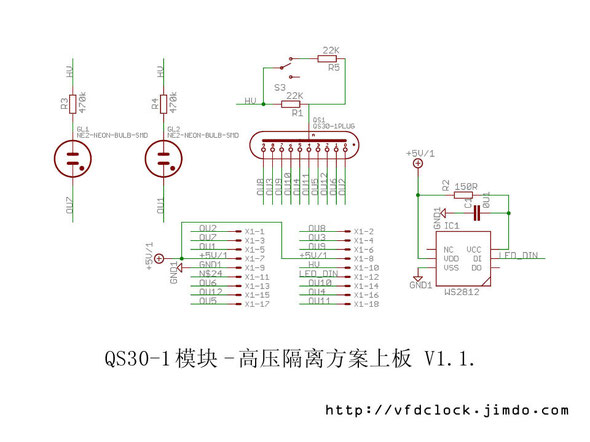
BOM表1
|
数量 |
元件值 |
名称 |
标号 |
|
1 |
2.0mm排针 |
87758-1816 |
X1 |
|
1 |
微型拨动开关 |
SWITCH-SPST-SMD-B |
S3 |
|
1 |
0u1 |
C-EUC0603K |
C1 |
|
2 |
22K |
R-EU_R1206 |
R1, R5 |
|
1 |
150R |
RESISTOR_EUR0603 |
R2 |
|
2 |
470k |
RESISTOR_EUR0603 |
R3, R4 |
|
2 |
NE2-NEON-BULB-SMD |
NE2-NEON-BULB-SMD |
GL1, GL2 |
|
1 |
QS30-1PLUG |
QS30-1PLUG |
QS1 |
|
1 |
WS2812 |
WS2812 |
IC1 |
BOM表2
|
数量 |
元件值 |
名称 |
标号 |
|
|
3 |
|
4R-N0603-ARC |
RN1, RN2, RN3 |
|
|
1 |
|
87758-1816 |
X1 |
|
|
1 |
|
CAP_TANTALUMB/3528_REFLOW |
C11 |
|
|
1 |
|
D-ZENERSOD123 |
DZ3 |
|
|
1 |
|
FE08W |
SV4 |
|
|
2 |
|
MA04-1 |
SWIM-IN, SWIM-OUT |
|
|
1 |
|
MA08-1W |
SV3 |
|
|
12 |
高压三极管 |
NPN |
Q1, Q2, Q3, Q4, Q5, Q6, Q7, Q8, Q9, Q10, Q11, Q12 |
|
|
4 |
0u1F |
C-EUC0603 |
C1, C2, C4, C5 |
|
|
1 |
0u1F |
C-EUC0805 |
C7 |
|
|
1 |
1k2 |
RESISTOR_EUR0603 |
R8 |
|
|
1 |
1uF/250V |
C-EUC1812 |
C9 |
|
|
1 |
3K3 |
R-EU_R0603 |
R5 |
|
|
1 |
3u3F/25V |
C-EUC0805 |
C12 |
|
|
1 |
10k |
RESISTOR_EUR0603 |
R7 |
|
|
1 |
10uF/25V |
C-EUC1206 |
C10 |
|
|
1 |
78SOT23 |
78S |
IC4 |
|
|
2 |
99 |
D-ZENERSOD123 |
DZ2, DZ4 |
|
|
1 |
100K |
RESISTOR_EUR0603 |
R3 |
|
|
1 |
150R |
RESISTOR_EUR0603 |
R9 |
|
|
1 |
270R |
R-EU_R0603 |
R4 |
|
|
2 |
680nF |
C-EUC0603 |
C3, C6 |
|
|
1 |
|
R-EU_R0603 |
R10 |
|
|
1 |
ER-TRANS-SMDER9/5 |
ER-TRANS-SMDER9/5 |
T1 ER9.5高压变压器 |
|
|
1 |
PNP |
PNP |
Q14 普通PNP三极管 |
|
|
1 |
SI2301DS-P |
SI2301DS-P |
Q15 PMOSFET |
|
|
1 |
SI2302DS-N |
SI2302DS-N |
Q13 NMOSFET |
|
|
2 |
STM8S103FXF3 |
STM8S103FXF3 |
IC2, IC3 |
|
|
1 |
TLP283 |
TLP283'SSOP4' |
OK1 |
|
|
1 |
US1M |
DIODE-SCHOTTKYSMA |
D3 |
|
|
1 |
VARISTORCN1206 |
VARISTORCN1206 |
FUSE1 自恢复保险丝 500mA |
|
焊接制作
电路零件组成部分并不复杂,基本构成就是两片SSOP20封装的单片机与变压器以及一些三极管等常规零件,所以焊接工作不会很困难,主要是要注意两片单片机的程序是不同的,不要焊接错了,其余的常规零件,应该很好焊接,只要注意焊接温度不要过高即可,焊接技巧请参考前几期的相关文章,这里不再重复。上板焊接QS30-1插座时,由于使用的是13脚的搭棚插座,建议焊接前插入焊孔量出所需长度,然后做上标记后用水口钳剪去多余插脚后再进行焊接,而且焊接插座前应先确保LED焊接正确,且最好先进行点亮测试无误后,方可焊接陶瓷插座,否则焊接完插座后再发生错误则拆焊工作会变得很困难。
由于涉及到高压应用,所以焊接完成后的电路板应该喷涂上电子三防漆加以保护。三防漆的主要作用的保护线路板免受坏境的侵蚀,喷涂后的三防漆在固化后可在PCB表面形成一层透明的保护膜,实现绝缘、防潮、防漏电、防震、防尘、防腐蚀、防老化、耐电晕等功能。一般情况下购买到的三防漆基本都是喷罐的形式,喷涂时建议先使用报纸或者胶带等覆盖不需要涂装的部位如接插件等部分,然后保持喷罐水平,距离PCB大约20CM左右的位置开始来回扫喷,确保喷涂层的均匀。喷涂完成后的电路板放在通风区干燥后即可使用。
安装注意要点
1、焊接过程应尽量使用恒温的防静电烙铁进行焊接,焊接时间尽量短,以防止损坏零件;本制作为了尽量缩小尺寸,选择的零件都是密集引脚封装,在焊接过程中如果有热风枪配合,可极大提高焊接效率;
2、焊接过程中应详细对照电路资料,确保零件焊接正确,在焊接过程中,可先焊接单片机与隔离电源部分,焊接完成后可先进行程序写入及上电测试,先确保隔离电源部分工作正常后再焊接剩余电路;
3、将高压部分电路放在最后焊接、调试,且在调试过程中应注意安全,在高压部分电路完成后的每次修补过程都需要在断开电源的情况下进行,以防止被电击;
4、焊接完毕,应对PCB进行仔细清洗,同时有条件的情况下可对PCB喷三防漆以防出现漏电问题,有可能的话,可在PCB高压部分使用高压硅橡胶进行密封,以提高安全系数;
5、本电路可调零件,只要零件质量过关,焊接正确无误且程序正确烧入,通电后即可正常工作;
6、更换NIXIE管时请在断电的情况下进行,以确保安全。由于管子与管座的制造精度均不是很高,所以应仔细对准后插入,不要使用蛮力以防止出现损坏。

软件层接口定义
由于本制作实现的是级联模块,所以设计上定义的数据流方向是由外部ARDUINO输出显示数据到第一模块,然后由第一模块处理后再通过模块的输出口输送给第二模块,依次传递数据到最后一块模块后完成显示功能。
在STM8S的硬件层上引出的是标准的SPI口,如果使用标准SPI口进行通讯,用户也可使用非级联方式实现独立片选或者SPI链的形式进行通讯。
由于SPI通讯由内部单片机硬件实现,在通讯方式上了无新意,所以本制作最后确定的软件层上未使用SPI接口规范,而是使用了一个HV5812数据兼容的模拟通讯层方案,也就是使用STM8S的IO口模拟HV5812驱动芯片的时序,说直白一些,就是使用单片机完成了一个串转并芯片的逻辑功能。
之所以使用软件模拟串转并芯片功能,而未直接使用SPI的原因是从实用性上考虑的,软件模拟串转并芯片的缺点是数据通讯速度比较慢,但是可以实现与HV5812直接级联,也就意味着我们这里制作的这个NIXIE模块不仅可以实现同类型模块之间的通讯,也可以直接与先前制作的基于HV5812的VFD模块通讯,兼容性比较好,而且数据格式简单明了,便于应用者理解,驱动代码只需要在先前ARDUINO驱动程序的基础上稍做修改即可。由于先前制作的VFD模块与本制作的NIXIE模块都由板上电路完成了LED与NIXIE管的灰度驱动,所以实际需要的驱动数据的刷新频率并不会很高,实测,ARDUINO驱动模拟串转并端口,可以做到1秒时间内刷新50次以上的显示数据,已经完全满足了实际应用需要。
通讯逻辑确定下来后,即可确定通讯数据,每个模块的通讯数据由LED显示数据与NIXIE显示数据顺序组成,其中前3个字节为8位的RGB灰度显示数据,后根的6个字节为12个高压显示笔段的对应数据,每个数据为4位,分别由一个字节中的高4位与低4位顺序组成,代表各NIXIE显示段的16级灰度值,数据传输完成后,在锁存脚上增加一个高电平脉冲即可将数据锁存入模块并立即显示出来。数据层结构与通讯电平逻辑是非常简单的,具体情况参考相关ARDUINO原代码。
|
数据 |
RED |
GREEN |
BLUE |
N1+N2 |
N3+N4 |
N5+N6 |
N7+N8 |
N9++N10 |
N11+N12 |
|
位长 |
8-bit |
8-bit |
8-bit |
4bits+4bits |
4bits+4bits |
4bits+4bits |
4bits+4bits |
4bits+4bits |
4bits+4bits |
表:显示数据参数表(发送顺序为高位在前)
NIXIE管的检测与修复
由于大部分NIXIE管的生产年限都是上世纪60年代到80年代之间,很多管子都已经生产了30年以上了,尤其是国产管,由于国内当时的技术条件限制,加上NIXIE管的工作寿命本来就比较低,国产NIXIE管的设计寿命只有1000小时左右,所以在制作时应该尽可能选择全新的管子,以确保显示质量与显示寿命。正常的QS30-1管子通电后应确保显示完整、清晰,均匀,除点亮的电极外,其余电极不应有发光现象。考虑到读者通过一些P2P采购渠道购买到的不一定是全新的管子,尤其是QS30-1硬管脚结构,旧的管子可以直接从管座上拔起,很容易并被商家充新销售,很难仅通过外观区分完好程度,所以导致电子爱好者现在通过市场采购到的很多国产NIXIE管都存在显示上的问题。最主要的问题表现在数字显示不完全,只能够显示局部,显示时辉光效果不均匀等,在使用前需要对管子先进行“修复”操作。
判断是否为新管子的简单方法是看显示面的阳极网罩是否有烧黑的痕迹,通常情况下的新管子前网罩折光看会有一层均匀的金属光泽,管子使用过程中的出现的老化现象主要表现在电极蒸散导致的管壳发黑,影响显示效果,使用过一段时间后的管子有明显的黑化痕迹,尤其网罩中心更加明显,视网罩黑化的程度可大致判断使用时间。
一般情况下,对于管子屏面严重发黑,上电后内部仅管脚区亮或者数字严重显示不全的管子可做放弃处理,而对于那些仅个别数字的局部无法完全点亮,而管子状态依旧较好的管子可进行修复处理。NIXIE管产生显示不全的主要原因是“阴极中毒”(cathode poisoning),修复的原理主要是使用高压驱动确保其尽量点两,然后利用增加工作电流的方式使金属表面发热后“活化”,经过“活化”处理过的笔段在降低到正常工作电压与电流后依旧可以确保完全显示。本质上所谓的“活化”过程的原理就是通过对管子显示阴极施加超过正常工作条件的电流,使其发热并维持一段时间,使其表面影响显示的局部的化合物层逐渐蒸发掉。
对于一些管子因生产质量因素或因保存时间过长等出现显示笔段显示短缺现象,可使用提高驱动电压的简单方法进行再次激活,这个方法的基本原理是从管子的额定工作电压开始在确保限流的前提下逐渐提高驱动电压,直接至管子笔端显示完整,并保持一定的时长(从几小时到几十小时不等),然后降低到额定工作电压看其是否能够正常显示。视管子的工作状态可再次进行以上操作步骤。对于电压提高到一定程度也无法完整显示的笔段,可考虑保持高的驱动电压,并且维持几小时时间,直至其能够完整显示即可。
业余条件下针对NIXIE管的简易修复方法也就是提高显示电压与工作电流并保持一定的时间,利用高电流使字符显示恢复正常。由于NIXIE管本身具有稳压特性,修复过程中提高电压的目的主要是尽量使显示不全的笔段尽量点亮,在确定修复电压后,可减小限流电阻,使其显示笔段表面发热。根据实际管子老化程度的不同,电压升高的程度与限流电阻可酌情增减,加电持续的时长也可以视实际需要灵活调整。
如果所需要修复的管子数量较多,可考虑制作一个专用的修复器,修复器电路网上即可搜索到,实际常见的修复电路就是一个输出电压可调的DCDC电源,通过串联不同的限流电阻完成修复工作。具体修复操作步骤为:活化电压从170V起缓慢升高,直至管内笔画显示完整,亮度显示均匀为止。然后降低电压到170V正常工作,看此管子能否依旧保持正常显示状态。大部分内部结构完好的管子在电压升高到250V~300V之间时,基本都可以完整显示(记得要在高压输出与NIXIE管之间串联一个50K~80K左右的限流电阻,防止损坏管子)。同一管子的不同数字段可能需要施加不同的活化电压,所以活化时建议逐字进行活化。即对于存在多个数字显示缺失的管子,分别对不同的数字段单独进行活化。经过活化操作的管子可在一定时间内恢复正常显示。
在活化过程中,可在管子加电的两端连接上万用表测量电压,正常工作的字段两端的电压基本稳定在150V左右,缺笔画或者存在其他显示问题的字段两端电压明显偏小,一般缺半字的笔段电压在130V左右,这一特点可以做为字段是否存在问题的一个可量化测量标准。
如果经短时高压活化依旧无法正常显示的管子,建议施加更高的电压并且维持更长的时间。实际操作时可直接使用高电压,在最高电压位置还是无法完全显示的笔段,可保持高压几个小时,再看是否能够拯救。一般经验是活化阶段电流最大不应超过5mA,电压不应超过300V为宜。实践总结的经验是3mA典型修复电流,260V电压的情况下,大部分的新管子都可以在短时间内被修复。一般的修复过程是通过增加工作电压,使笔段基本被点亮,然后维持一段时间,等笔段所有区域全部连为一体后,降低到正常工作电压,看看此时笔段是否已经正常,如果还未正常,则重复上述过程。通常视管子的具体情况,修复过程可能需要几分种到几小时不等,对于高压点亮超过24小时都无法修复的管子,可以做放弃处理。在修复过程中还要特别注意高压的掌握,电压升高后,一些不应该被点亮的部分如管子内部的管脚部分也有可能被点亮,此时应该降低电压,否则如果保持这种供电状态,最后修复完成的管子的管脚引线部分也会持续发光,甚至出现只有管脚引线发光而数字不发光的现象。
考虑到业余爱好者自制修复器比较麻烦,所以在本模块的设计中考虑到了这一应用需求,在模块上增加了一个倍流开关,可实现简单的修复工作。实际上,本模块的默认输出驱动电压可达250V,完全满足基本的修复电压需求,而在显示管所处的上板增加了一个倍流开关,可将另外一个附加的电阻并联到原限流电阻上,可实现倍增输出电流的功能,实际修复测试过程中,对于一个8字笔段只显示一半的NIXIE管,施加倍流电压,连续工作3小时后,8字笔段原不显示的部分逐渐愈合显示,维持5小时后,显示完全恢复正常,实际修复过程中可以配合外部ARDUINO的程序,实现在修复过程中,较长时间点亮待修复字段,并且间隔一定时间后轮流循环显示一轮全部字段,通常只要不是特别严重的显示问题,都可以在12小时内恢复正常,当然在修复过程中,如果发现管子不应发光的引线部分也发光了,表明电压过高,则建议立即停止修复过程。
NIXIE管毕竟是年代非常久远的显示器件,目前能够采购到的管子实际显示效果都不会太好,所以先要有心理准备。当然,也可以考虑在硬件与软件层上做一些改进,例如对于老化的NIXIE管,在正常显示过程中,使用超过正常工作电压一定程度的高压但是配合不同占空比例的脉冲进行显示,这样一方面高电压可确保管子的正常显示效果,其次使用非100%的占空显示脉冲又可以防止管子因超压工作烧毁,是一个可选的显示方案。或者通过增加限流电阻的阻值降低Nixie管的电流,以确保长时间工作的寿命。同时在显示过程中应该注意不应使单一显示笔画长时间点亮,而应在点亮一段时间后,间隔一段时间就对全字段进行依次轮流显示,以确保管子的工作状态良好,不出现长时间未点亮的笔段出现显示不全等问题。
制作总结
本制作是本人设计并实践的第一个NIXIE管作品,期间经历了多次的实验、反复的失败、改进与调试过程,最终成功完成了本制作。总体来讲,整个设计调试过程就是一个学习知识与积累经验的过程,有辛酸也有喜悦。最后希望通过此篇文章能够与广大电子爱好者交流学习,共同提高电子制作水平。同时再次提醒一下,涉及到高电压的电子制作需要特别注意安全,本制作虽然使用了全隔离方案,极大地提高了安全性,但是当手指同时接触到内部的高压两极时,依旧存在电击危险,所以整个模块完成后,一定要使用亚克力外壳保护起来,以防止出现安全问题。
(全文完)
Wed
29
Jan
2014
为Arduino设计的IV-11通用荧光数码管模块
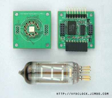
本文为版权内容,文章内容(包括但不限于文字、图片、声音、录像、图表、软件、程序)未经版权人书面许可,任何人不得引用、复制、转载、摘编或以其他任何方式非法使用。
Copyright material!
All material on this page is copyright of ZhangFeng(zjjszhangf@gmail.com) unless otherwise acknowledged. Duplication or sale of all or any part of it is not permitted.
作者:张锋 (zjjszhangf@gmail.com)
本制作的特点
1、 使用通用型电路设计,将电源供应与逻辑驱动部分分离成上下两块电路板,可在不更换底逻辑电路底板的前提下,适配多种不同的荧光数码管显示模块,具备极强的通用性;
2、 使用极高效的微型驱动电路,生成驱动VFD管所需的灯丝电压与高压,完全符合VFD屏驱动规范,电路尺寸小,转换效率高,显示效果优良;
3、 全板采用微型贴片零件制作,整机PCB只有3.5cm*3.5cm,板上驱动电路部分最高的零件高度仅为2.0mm,具备超薄型优势;除接插件外,其余全部零件都藏于模块中,整体模块外观简洁;
4、 模块设计使用无单片机驱动方案,无需程序写入器等设备,用户自备Arduino或其他普通单片机即可驱动,通用性强。
5、 制作容易,无需特殊调试,仅用一只普通万用表测量相关电压即可,适合初级电子爱好者自制;
6、 公开源码的驱动程序,使用纯C语言进行编写,可在Arduino平台上使用,也可很方便地移植到其他单片机平台上使用;
7、 整个模块自主保持显示状态,彩色LED部分自主支持真彩色灰度显示,可以出显示出RGB24位真彩色,显示色彩丰富,且无需单片机主动进行PWM扫描,用户程序仅需将所需显示的数据送入模块即可,节约大量单片机资源;
8、 整体所有接口引线全部通过插针引出,可根据实际需要进行多极极联结使用,每级输出的数据信号都经过板上电路放大后输出,确保了多极极联信号的稳定传输,无论极联多少模块,实际单片机的接口引线最少仅需3根,节约单片机I/O口资源;
9、 专门设计的亚克力外壳,不仅美化作品的外观,而且使用隐藏式的左右级联亚克力板配合螺丝组合,可以实现任意数量的模块连接,无需使用其他连接辅助板;
设计思路简介
本制作的设计思路主要是分析了常见的一些VFD显示管如:IV-11、YS9-3、YS9-4、YS30-1、YS27-3等的技术参数后,发现这些管子的都具备一些共同的特性,通过分析和利用这些特性,完全可以设计出通用的驱动电路模块。
首先,大部分的VFD显示管的尺寸都比较小,灯丝电压也不高,一般都在2V以下,由于灯丝电压低,灯丝两端的电压压降的差异所导致的与高压之间的电压差也比较低,大部分管子的灯丝驱动部分都可以自由选择使用交流或直流电进行驱动而不会出现显示亮度差异的问题。同时个别尺寸较大的管子如IV-11显示管,因管子内灯丝斜拉补偿的原因,只能使用直流电驱动,如果使用交流驱动则会导致管子显示面上下亮度出现明显差异。综合以上技术信息,可以确定通用的灯丝驱动部分可选择使用直流电进行驱动。
其次是高压部分,驱动这些管子的高压部分的电压范围大致都在20V~30V之间,如果是正高压驱动,这样的高压在使用5V为主供电的电路中,使用一个简单的Boost DC/DC升压电路即可很容易地生成,这个部分电路比较简单,现成的芯片也很好买,成本也低。
就笔段数量上来看,通常的8字VFD显示管的主显示笔段为7段,部分管子在显示区增加了右侧的[-]与[.]号,总笔段增加到了9段,除非是特殊的显示管(如米字管等),大部分的8字显示管的笔段驱动引脚数都不超过10个,所以可以考虑以10段作为上限,设计驱动电路。
在模块的驱动设计上,考虑到成本及组合需要,应该将模块设计成每个单独模块都能够完全独立工作,各级模块之间仅使用插口连接,完成主电源与数据信号的传递工作。在一个单管独立模块的设计上,由于只有一个单独的管子需要驱动,所以使用正高压配合直流灯丝且以静态驱动的形式是最合适的一种驱动方案,这一方案的优点主要是正高压与直流灯丝电压都很容易生成,而且基于VFD管的阳极熄灭法特性,在非扫描驱动的情况下,无需要使用负压Ek,所以灯丝与正高压之间完全可以共地,电源电路部分设计将简单很多。使用正高压驱动电路的缺点是与负压驱动电路相比,需要使用正压驱动芯片或者是使用双三极管进行电平移位驱动,零件成本成本会高一些。
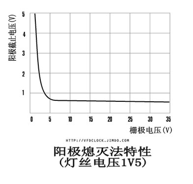
在模块的信号类型与极联设计方式上,考虑到模块所需的实际数据量很少,包含VFD显示及其他数据在内,一般都只有几个字节的数据量,同时考虑到需要简化与Arduino等驱动电路连接,所以在数据接口的设计上应尽量考虑减少连线,最后决定使用串行类型的接口作为信号接口。
与VFD TUBE电子时钟等的制作类似,可以在VFD管的下方增加RGB真彩色LED作为底部光源,以加强模块的实际显示效果。实物也可考虑同时使用透明亚克力板等设计对应的面板,利用亚克力板的侧面导光性,在制作的外边缘生成一层彩色灯光亮边,提升制作的实际显示效果。
由于大部分8字荧光数码管的驱动要求都基本一致,都需要灯丝电压与栅极与阳极电压,仅电压类型与电压值有差别,这里仅以IV-11荧光数码管作为本例的范本,完成一个完成的模块制作,其他类型的显示管的制作原理是一致的,仅需重新设计上连接板即可。
下面先来了解一下IV-11荧光数码管的基本情况与电气参数。
IV-11(ИB-11)数码管简介
IV-11荧光数码管为上世纪90年代乌克兰生产的真空荧光显示管,直立安装侧面显示。管内包含一个标准7段数码加一个小数点共计8个显示笔段,笔段发光颜色为亮绿色,显示效果较好。IV-11荧光数码管的主要优点是管子尺寸比较大,数码管整体高度60.0mm直径22.5mm,其中内部笔段显示区域高度为21.0mm,宽度为14.65mm,显示区与传统荧光显示管相比要大很多,显示效果也自然更加醒目,所以经常被也爱好者用来制作成时钟应用。
全管总计11只管脚,管脚直径为0.5mm,其中Pin1与Pin11脚为灯丝引脚,Pin2脚为栅极引脚,其余8脚为笔段阳极引脚。引脚功能详见下表。
|
引脚 |
11 |
10 |
9 |
8 |
7 |
6 |
5 |
4 |
3 |
2 |
1 |
|
功能 |
灯丝F+ |
Grid |
E |
H |
F |
A |
G |
B |
C |
D |
灯丝F- |
IV-11原始说明书为俄文,可以通过网络搜索到译为英文的说明书。从说明书描述的电气参数来看,它的供电结构比较简单,灯丝工作电压Uf为1V5,栅极电压Ug与阳极电压Ua电压值相同,在静态显示模式下,推荐的电压值为25V~30V,在动态显示模式下推荐的电压值为50V~70V,最高电压不应超过70V。从电流参数上看,此管电流消耗较大,灯丝部分典型工作电流If为100mA,高压部分中栅极典型工作电流Ig 为12~17mA,阳极典型工作电流Ia为3.5~5mA(单一阳极平均电流为0.8mA),与其他类型的显示管相比,此管接近一半的功率消耗在驱动栅极与阳极上。应当特别注意的一点是IV-11荧光数码管属于直流管,其灯丝电压为直流驱动,如果从侧面观察管内灯丝位置情况,可发现灯丝是斜拉式安装,通过灯丝与显示面的距离不同来对直流电位差进行补偿。就补偿的原理来分析,灯丝距离栅极较远的一端为应为负极,灯丝距离栅极较近的一端则为正极。这一点其实很好理解,灯丝负极与共地的栅极高压之间比灯丝正极与高压之间具备更大的电压差,如果要维持均匀的显示亮度,灯丝负极距离显示区的位置自然更远一些。所以在实际应用时,灯丝供电的正负极千万不要接错,也不要使用交流电压来驱动灯丝,否则数码管会出现显示时文字上下亮度明显不一致的现象。
从外观上来看,IV-11为典型的侧显管,即管子的显示面在侧平面上。此类管子的安装方式一般采用沿PCB平摆安装或者垂直安装为佳,通常制作成电子时钟应用时,采用的都是垂直直立焊接方式进行安装,本制作也采用此种安装方式。观察管子的内部,其总体结构还是比较简单的,属于典型的真空三极管式荧光显示管,内部垂直走向的灯丝及网格线型的栅极组成了基本的驱动结构,阳极笔段电极通过背板后的引线引出连接,内部连线清晰可见。但是从管子的整体做工上来看,工艺略显粗糙,虽然生产年代仅仅在十几年前,但是依旧有一部分的管子内部金属板部分还是有明显的班驳老化的痕迹。在实际测试中,还发现个别荧光管连接栅极高压后,屏幕上出现明显的红色辉光的现象,小部分管子的品质算不得优异。所以在实际使用前,应该先使用测试电路对管子进行筛选,剔除瑕疵品。筛选过程中尽量选择显示品质接近、无明显异常、管子内部金属板颜色一致、工作状态良好的管子成组使用,以期在多管串联应用中获得良好的显示效果。
对于VFD荧光显示管,典型的快速测试可以直接使用普通电池来供电,其中灯丝部分使用一节1.5V的干电池供电,高压部分可使用两节或三节9V层叠电池串联后供电,两组电池共地连接。电池与显示管的连接可使用杜邦线或者鳄鱼夹进行,先将1.5V电池连接到灯丝引脚,正常情况下,灯丝会发出微红的光,表示灯丝工作正常。然后将共地的高压部分连接到栅极与各阳极引脚,即可使笔段发光,仔细观察显示效果与笔段发光的均匀度,尽量选择显示优异的管子备用。

荧光管供电电路设计
荧光管供电电路设计中先要确定驱动方式及供电方式,驱动方式传统上有动态驱动与静态驱动两类,其中动态驱动的优点的引脚少,线路连接容易,但是显示时容易产生闪烁感,且动态显示时所需要的驱动高压已超过安全电压范围,存在触电的危险,而静态驱动虽然需要更多的驱动引脚,但是显示稳定无闪烁,对高压的要求也比较低,同时另外一个显著的优点是,由于IV-11的灯丝为直流供电,且电压只有1.5V,在静态驱动的情况下,对截止偏压无要求,可以直接将灯丝与驱动高压共地连接,极大地简化了两组电压的连接关系。而且本制作设计成单一模块组合连接方式,如果使用动态驱动则Grid部分的引线连接不是很方便,所以最后决定选择使用静态驱动方案。
供电方式可选择的方案为正压高压与负压高压,使用正压高压的优点是容易生成,市场上有很多专用的电路可以直接生成大电流的正性高压,方案成熟,缺点是使用正压VFD驱动芯片的价格可能是负压驱动芯片的好几倍,价格较高。使用负压驱动的优点是VFD负压驱芯片价廉且易购,缺点是大电流的负压生成不易,传统上采用高频变压器的方式来生成,效率不高。考虑到IV-11的灯丝采用直流电进行驱动,使用负高压则需要使用变压器进行隔离,会造成电路设计复杂化,所以本制作选择使用正高压配合专用的正高压驱动芯片完成管子的驱动。虽然驱动芯片价格稍高,但是正压电路的成本降低了,综合起来元件总成本提高不多。
驱动IV-11需要提供两路基本的供电电压,分别是灯丝电压与驱动正高压,下面分别对这两组电压的电路进行说明。
灯丝电压规格为为直流1.5V,单管工作电流为100mA。在主供电为5V直流的情况下,为了获得灯丝供电需要1V5的直流电压,需要降压电路进行降压,由于灯丝是阻性负载,则降压最简单的方法是在灯丝上串联一个功率电阻,或者使用LM317类可调节三端稳压电路进行降压,但是考虑到灯丝电流有100mA,以上方法效率很低,大部分能量都发热浪费掉了,所以本制作最后选择使用专用的DC-DC降压芯片组成Buck电路,以提高灯丝供电效率。考虑到制作布线的简洁及PCB面积的限制,同时考虑到市场实际的采购情况,实际选择的降压芯片为SOT23-5封装的1.2M高频Buck芯片完成降压电路,此类芯片大部分著名的半导体公司都有管脚兼容的产品,所以可根据自己的实际情况自行选择具体的型号。这个电路基本都可以提供300mA以上开关电流,而且电路转换效率都在90%以上,同时由于是高频转换,所以可以使用体积极小的功率电感,占据PCB面积极小。对于1V5定压应用,可选择使用定压规格的Buck芯片,可节约外部的采样电阻,外围零件只有电感与输入与输出电容组成,灯丝供电部分的整体线路简单明了。
对于高压部分,由于本制作是使用正高压进行驱动,电压范围为+25V~+30V,所需的驱动电流也比较小,最高电流约为20mA左右,对于这样的电压生成,使用市面上大部分公司生产的SOT23-5封装的Boost芯片都可以生成。选择时只需要重点注意一下Boost芯片的最大开关管耐压应在30V以上才可使用。Boost电路结构是通用型电路,由Boost芯片驱动电感后经肖特基二极管整流后输出,反馈电压使用两电阻组成的电压采样电路返回到Boost芯片的FB引脚。这种升压电路很常见,细节部分这里就不再详细说明。

以上供电电路的注意点主要集中在PCB线路布置上,对于高频DC/DC转换电路的元件选择及布线一般需要注意一下几个要点,以确保电路工作稳定。
1、电感应选择高Q值的功率电感,为防止对周边电路的干扰,最好选择磁屏蔽电感,电感下方应覆地平面,不要走线;
2、输出电容尽量选择低ESR的钽电容或陶瓷电容,位置尽量靠近Buck/Boost芯片输出脚;
3、尽量增大地平面的面积,减少线路损耗,避免元件发热;
4、二极管应选择耐压足够的肖特基二极管,可以提供较低的正向压降及快速的开关速度;
5、如原厂提供PCB建议布线图,应尽量采用,以期获得稳定的工作电路与高效的转换效率;
模块驱动电路设计
基本设计上考虑,模块的底板应该是通用的,应完成数据通讯、显示管驱动、LED驱动、电源供应等功能,而模块的顶板则放置LED管、VFD显示管,且应该是可更换的。在这个模块的前期测试电路的设计中,原本为了确保节约成本,将大部分驱动零件都位于底板上,包括了电源电路,而顶板仅有一只RGB-LED与显示管。但是在实际应用中发现的问题是虽然可以通过底板上的开关/跳线调整出几组不同的灯丝电压与高压,但是方便性不足,同时由于没有对应的显示板类型判断电路,所以很有可能将不正确的电压施加到不同显示管模块上,虽然电压差异都比较小,不足以烧毁显示模块,但明显欠缺通用性与灵活性,用户使用起来也不方便,更换模块时需要特别注意电压跳线。经过改良,最后确定的电路板结构中,将灯丝与高压电路放到了显示板上,由显示板提供对应管子配套电压电路,并且将正确的高压由显示板传递到底板上使用。这样的设计的主要缺点是增加了成本,每个显示板都需要一套对应的电压生成零件,但是优点也很明显,一来不会因为显示模块的切换而需要改变驱动电压,因为驱动电压是固定在显示板上的,同时高频生成电路均位于顶部的显示板上,对于底板通讯电路的影响比较小。从整个模块的结构上看,使用这样的设计也充分利用了两板之间的空隙,减小了模块的总高度。
对于模块的数据接口,传统的设计思维是使用74HC595等芯片作为串并转换电路进行信号的极联,74HC595的端口可以直接驱动小型的RGB LED,而VFD的阳极部分的驱动则在74HC595输出口上增加电平移位电路进行驱动,通常是使用NPN+PNP组成一个标准的电平移位电路或者直接使用三极管阵列(如:TD62783)芯片完成这一工作。当然,如果对工作效率没有太大的要求,追求使用较廉价的零件,以上电路也可以仅使用一只NPN三极管或者同类的廉价三极管阵列如ULN2003组成“短路型”电路进行驱动,可节约成本。
上述电路的优点是74HC595价格低廉,电路结构简单,容易驱动。缺点也很多,首先从LED驱动上来看,由于仅仅是使用简单的串并转换,点亮RGB-LED是没有什么问题,但是要根据用户需要形成绚丽的灰度效果,只能由用户单片机主动进行PWM刷新工作,这样不仅大量消耗用户单片机的资源,同时也因为简单的PWM驱动由于速度的限制,很难形成稳定的真彩色效果,而且随着模块极联数量的增加,每次传递的数据量也会成倍增加,效果更是要大打折扣。其次是74HC595无法直接驱动VFD笔段,使用三极管等转接驱动大大增加电路的成本与焊接工作量,而且自家PCB尺寸与布线难度。所以以上两个驱动工作应该考虑选择专用的驱动电路且最好两者之间能够直接连接的芯片进行驱动。
经过多次的选型与试验,最后选定使用以下两种芯片进行驱动:对于LED驱动部分,选择使用台湾点晶公司生产的DM413芯片作为三通道RGB-LED的驱动芯片,这个芯片的优点是提供8位、13位、14位可选的灰度驱动模式,其中8位模式为无gamma校准的rgb-24位模式,13位模式为5字节数据,RGB每位带5位gamma校准数据,而14位则为4字节数据,RGB数据后带一6位全局亮数据格式。使用以上任一格式都可以显示出绚丽的RGB色彩。此芯片的接口是典型的串行SPI类的接口,驱动简单,更加值得一提的是,由于原芯片专门就是为LED级联设计的,所以在芯片上提供了独立的信号输出端,级联信号通过芯片内部重整后在特定输出口输出,以确保传递给下一级的信号的稳定。同时对于输出的数据信号的触发沿类型等参数可通过引脚来进行设置,具备极强的通用性。
在高压驱动芯片的选型上,考虑到与LED驱动芯片的直接连接,最后选择了Supertex公司出品的HV6810,此芯片为串行接口型串入并出高压转换芯片,片内总共提供了10只高压输出引脚,高压部分典型支持电压为20V~80V,是专为VFD驱动设计的高压驱动芯片。虽然芯片价格高一些,但是单片即可完成所有VFD引脚的驱动工作,大大减少了元件数量,也降低了电路设计的复杂度,所以选用这一芯片还是值得的。HV6810与DM413之间可以数据信号直连,在电路设计中考虑到需要利用DM413的数据输出重整功能确保传输给下一级的数据信号的稳定,所以在连接上,将HV6810数据口作为主接收口,HV6810输出的数据再连接到DM413上,最后经过DM413重整后输出的数据传输给下一个模块,确保了信号传递的稳定。HV6810与DM413仅在锁存信号的极性上不相同,这个信号使用一个带阻的NPN型数字三极管构成一个反向门电路进行反转,具体连接请参考本制作的电路图。
供电保护电路
由于受到模块PCB面积的限制,本模块没有设计过压保护电路,所以在输入电路的电压上需要特别注意不要出现过压的情况,通常输入电压最高不应超过5V5。
为了保护模块,电路中使用1206封装的自恢复保险丝作为过流保护器件。同时为了防止出现电源反接造成电路损坏,还在电源电路中增加了反向极性电压保护电路。通常在对电压压降不敏感的电路中,可串联一个低压降的如SS14肖特基二极管作为反接保护元件,优点是简单,缺点是二极管上存在压降,易造成功率损耗。而本模块需要提高效率,保持低压降,所以这一反接保护电路使用一个门极接地的P沟道的MSOFET管来实现,电路利用PMOSFET极低的导通电阻来提高电路效率。
电路图及零件表
经过多次优化后的整体电路设计简洁明了,电路中分成上下两部分模块板,中间使用2.0mm的排针与排座位进行连接。模块之间使用8pin的单排2.54的排针与排座连接,主要目的是增加连接的可靠性。其中电源输入与地部分各使用了其中的两脚,以减少供电的接口电阻,确保供电的稳定。
实际测试结果表明,整个模块电路工作稳定,板上零件在正常工作状态下长时间连续工作也无任何发热现象。VFD管显示亮度高,各字段显示亮度均匀,无闪烁。
底板元件表:
|
数量 |
元件值 |
元件名称 |
元件标号 |
|
1 |
|
87758-0816 |
X2 |
|
1 |
|
87758-1016 |
X1 |
|
1 |
|
C-EUC0805K |
C7 |
|
1 |
|
DTC114EKA-10K-10K |
T |
|
1 |
|
FE08W |
INPUT |
|
1 |
|
MA08-1W |
OUTPUT |
|
5 |
|
RESISTOR_EUR0805 |
R1, R7, R8, R9, R10 |
|
1 |
|
SOLDERJUMPER_2WAYS |
SJ1 |
|
1 |
|
VARISTORCN1206 |
R6 |
|
2 |
0u1 |
C-EUC0805K |
C6, C8 |
|
1 |
DM413SOP16 |
DM413SOP16 |
IC3 |
|
1 |
HV6810SW |
HV6810SW |
IC4 |
|
1 |
SI2301DS-P |
SI2301DS-P |
Q1 |
IV-11顶板元件表:
|
数量 |
元件值 |
元件名称 |
元件标号 |
|
1 |
|
87758-0816 |
X2 |
|
1 |
|
87758-1016 |
X1 |
|
1 |
|
BAV99SOT23 |
D1 |
|
1 |
|
CPOL-EUB/3528-21R |
C1 |
|
1 |
|
IV-11BIGHOLE |
VFD |
|
1 |
2M |
RESISTOR_EUR0805 |
R1 |
|
1 |
2u2h |
INDUCTANCE_US3*3 |
L2 |
|
1 |
4u7 |
C-EUC0805K |
C4 |
|
1 |
4u7/25V |
C-EUC0805K |
C2 |
|
1 |
4u7/50V |
C-EUC0805K |
C3 |
|
1 |
10u |
C-EUC0805K |
C5 |
|
1 |
22p |
C-EUC0805K |
C6 |
|
1 |
10uH~22uH |
INDUCTANCE_US3*3 |
L1 |
|
2 |
100k |
RESISTOR_EUR0805 |
R3, R4 |
|
1 |
150k |
RESISTOR_EUR0805 |
R2 |
|
1 |
LED-TRICOLOR-5050 |
LED-TRICOLOR-5050 |
LED1 |
|
1 |
LED-TRICOLOR-THROUGHHOLE |
LED-TRICOLOR-THROUGHHOLE |
U$1 |
|
1 |
LED-TRICOLOR-THROUGHHOLESMALLHOLE |
LED-TRICOLOR-THROUGHHOLESMALLHOLE |
LED |
|
1 |
LT1613 |
LT1613 |
IC2 |
|
1 |
LTC3406B |
LTC3406B |
IC1 |
安装调试
由于本制作设计中分为上下两块板,建议先焊接底板。底板上包含两大片的集成电路,可先焊接上,由于两芯片是SOP封装的,所以在焊接上不存在什么难度,只要注意在焊接时确保引脚与焊盘正确对齐即可。一般是推荐在焊接前,先焊上边缘一脚先完成对位固定或者使用耐高温胶布在板上固定元件。底板左右两边的8-pin的排针与排座应尽量贴紧PCB后方可进行焊接,一般建议先使用夹子夹紧后再焊,以确保模块左右级联的平整性。有条件的情况下,可考虑在排座下方贴3M强力双面胶纸,以确保排座保持水平。
特别需要注意的是使用的2.54单排针应该使用单排反弯针,如果采购不到,也可以自己制作,方法是将双排弯针的短针拔出,反插到普通单排针的塑料件内,然后使用排座插入,推平对齐即可。
在自制反插针时,最容易想到的方法是使用尖嘴钳等工具将插针拔出,实际这不是一个好方法,强行拔针容易造成插针弯曲报废。实际推荐的方法是将插针前端顶着如木块等硬物,然后前推插座塑料件,将插针从后部推出即可。这种方法可以获得完整不变形的插针。
在回插插针时,应该特别注意插件塑料件平整一面为向外的一面,不要弄错了。插针插入塑料件后,先不要去关注对齐问题,可先将插针插入PCB安装孔内,然后使用一单排座,插入插针头位置,均匀使力,即可推平插针。
单排反插针具体制作过程如下图。
上下板连接排针与排座必须焊接平整,防止插接时出现歪斜,一般推荐先在底板上焊接排座,焊接无误后插上排针后再放上上层PCB后进行焊接,这样可确保上下板的对齐。
由于上板包含了灯丝电压与高压部分的电路,所以上板可单独进行调试,方法是在焊接完两组DC/DC转换电路后,通过插针为上板供电,然后测量两组DC电路输出电容两端的电压,即可判断两电路是否工作正常。特别注意的是,测试前需要将排针中En对应的引脚连接在正电压上,使用一个2.0mm的短接插头即可(实际使用2.54mm的短接插头也可以)。
如果上板各组电压生成正常,底板无短路等问题,即可组合上下板后进行测试,由于上下两板分离式设计,所以批量制作时,可分开调试,简化了调试工作。
由于IV-11目前价格较高,采购不易,为确保IV-11型VFD管的可重复利用性,本制作使用了插座法进行连接,对于没有成品插座的管子,选用标准的插座针进行转接。焊接插座针时,应先将插座针套在管子引脚上,尽量确保插座针开口位置的对称,以确保成品的美观性。排列整齐后,连管子一起插入PCB对应的焊孔内进行焊接。焊接时需要特别注意焊锡的用量,不要让焊锡通过缝隙进入到插脚内,造成插座针报废,或者在焊接前先使用茶色耐高温胶带先将插座针顶部保护起来。完成焊接后的插座针尾部细脚部分过长,会影响上下板的组合安装,所以在焊接完成后需要使用水口钳将超长部分剪去,在不影响模块安装的前提下,尽量在末尾保留小段的细脚部分,以保持模块的美观。
由于使用了高效的DC/DC转换模块,所以本模块的电源转换效率相当的高,通常为90%左右。高效的转换节约了电力消耗,使得模块的工作电流相对较低。实测驱动一个IV-11显示板的VFD模块,在5V供电条件下,全点亮VFD所有笔段外加全点亮板上5050-LED部分的总实际电流消耗通常在140mA左右。其中大约2/3的电流是消耗在点亮IV-11上,大约1/3电流消耗在LED上。可见在这一模块中IV-11是主要的耗电大户。通常情况下,如果以一个标准的电脑USB口供电,电流不应超过500mA,则一个电脑的USB口的电力大约可以驱动3只串联的IV-11模块,如果需要串联更多的IV-11模块,则需要考虑使用双USB口或者使用单独的电源适配器供电。视实际使用的VFD管特性及点亮笔段的不同,电流可能有一定程度的加减,但是如果发现电流超过200mA,则应仔细检查线路及所使用的零件质量。
如果换用如YS27-3等小耗电量的VFD显示管模块板,实际整体模块工作电流可以减少一半以上,可以在同等电源功率下串联更多的显示模块,具体视所使用的管子类型及实际耗电情况确定。
由于模块使用单一5V外部供电,通常少量使用的情况下,可以使用ARDUINO UNO板为模块供电。当串联模块过多,所需电流过大时,可使用外部电源适配器为模块供电,同时模块引脚中包含两组的电压引脚,其中的一组可以引出电源为ARDUINO UNO板供电。
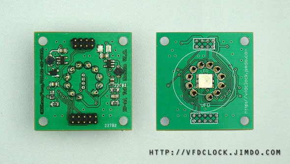
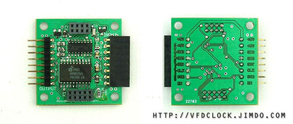

数据接口及软件层应用
本模块的数据接口层比较简单,就是通常的SPI接口,根据所选择的DM413工作模式的不同,有不同的数据流格式,但接口本质是不变的。每个模块的数据包含LED使用的RGB真彩数据与可选的gamma数据,后跟10位的VFD数据。根据DM413三种工作模式,分别是5字节的13-bit模式,4字节的14-bit模式及无gamma的3字节8-bit模式的,以上三种模式可通过PCB底板上的短路接头及焊盘完成设置,其中焊盘拉高与拉低选择其中两种模式,最后一种模式使用焊接>100pF容量的电容来完成第三态模式的选择。具体请参考电路图及DM413的说明书。
由于本制作对LED的色彩精确性的要求不高,考虑到减少数据量及保持通用性,没有使用gamm数据,默认使用的是24-bit的3字节DM163工作模式,LED数据结构为通常的R8G8B8模式数据结构。
为便于操作模块中各种不同的数据,在驱动代码的实现上,使用了一个C语言的结构来构造模块的数据体,具体结构定义如下,其中的vfdseg部分的uint16中的低10个位对应HV6810的10个输出引脚,数据结构的后部3字节数据则为24-bit结构的DM413中对应的LED数据。对于多个级联的模块结构,只需要使用一个这样的数据结构数组即可方便地进行定义整个连接的模块串中的各模块的对应数据。设置时只需要使用send_data()函数直接送出对应的数据数组即可,整体使用上非常方便。
实际数据传输部分的实现代码比较简单,按照接口的时序,逐一送出对应的数据,然后锁存显示即可。模块中的EN引脚用于关断模块内的灯丝与高压部分的工作,以节约电力,默认情况下无需连接。

驱动其他类型的VFD显示管
由于是模块化设计,所以本制作的底板可以驱动大部分的VFD显示管,在更换VFD显示管的型号时,只需重新设计一片简单的上接显示板即可,底板电路可以保持不变。
根据实际设计经验,一些如YS30-1、YS27-3型的显示管由于底部中心存在玻璃气孔管,所以在可能的情况下,尽量选择使用对应的插座,以方便在管子下方安装贴片LED。市场上YS30/QS30兼容的陶瓷插座比较便宜也很好买到,而YS27对应的插座则因价格较高,可以考虑使用插座针来转接,使用插座针的优点是插拔容易,缺点是会增加模块的整体高度。如果需要降低模块高度,也可考虑直接将管子焊接到PCB上,此时在设计上接PCB时必须考虑在转接板中间开孔,便于气孔管插入。同时应考虑使用多个微型的0805
RGB-LED取代通常的5050LED模块安装在VFD管底部的前后侧,以确保亮度均匀。
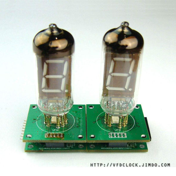
外壳设计与多模块连接
考虑到制作的美观,与多模块连接的需要,在制作后期,专门为此模块设计了配套的亚克力外壳,考虑到成本及模块尺寸,实际的外壳并非由完的封闭模块组成,而是由几片设计好外观的亚克力片组成,主要目的是提供一定的外观美观度与隔离裸露的电路板。亚克力主要遮盖模块的上下两面,由于PCB的外面都存在插针的焊点,所以应在亚克力对应位置处开孔,同时上板应使用透明或者半透明的亚克力材质,可以同时起到导光的效果,增加美观性。而下板则建议使用全透明的亚克力板,便于观察下板PCB上的各接口文字说明。

关于连接部分,原本考虑的是制作背板连接,即由预定义模块的长度,根据各模块的实际位置在背板上开启安装孔,然后通过模块上的螺丝将所有模块连接后统一安装到背板上。这一设计的优点是简单容易,而且背板设计安装在模块的背面,不占用模块的PCB空间。缺点是只能定制模块数量固定的背板,而不能随意级连,灵活性不足。所以最后的连接件的设计淘汰了固定数量的背板设计,而更换为左右连接的上板设计,即使用3mm厚度的亚克力板设计出左右连接的安装固定孔,在模块上板的下方空间内完成左右模块的连接工作,这一设计的优点是组合简单容易,可根据需要随意连接出任意长度的模块,花费的成本低,拆装方便。
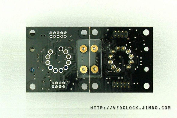
制作总结
本制作给读者提供了一个极通用的VFD数码管显示模块,作为对VFD管驱的一个实践性制作,配套上亚克力外壳,足以做成一个优质的Arduino模块使用。利用这一模块,Arduino爱好者们可以直接使用IO口驱动VFD,无需考虑复杂的灯丝、高压、LED扫描细节,可将更多的精力放在应用程序开发上。
希望这一文章能够起到抛砖引玉的作用,使更多的爱好者能够利用这一电路开发出更多的Arduino应用模块,并著作出自己的精彩应用。本文相关软件、硬件资料及后期开发进度,请关注本人的电子DIY博客——http://vfdclock.jimdo.com。
全文完

Sun
22
Dec
2013
IV-11 六管电子钟标准版套件制作说明

本文是针对IV-11六管电子钟套件(标准版)编写的制作说明。此版本套件的特点是标准管间间隔,尺寸比例恰当,适合桌面应用。通常情况下,此版是针对不安装管对间冒号器件设计的,但是在PCB上依旧保留了相关的安装位,如用户觉得有必要,依旧可选安装LED或IV-15器件作为冒号显示,最后只需在黑色的上板对应位置处使用电钻开孔即可。
此版本的套件在主要做了以下几点改进:
1、扩展了亚克力外壳尺寸,目前的尺寸已扩展为:230mm*65mm*75mm;
2、加厚了亚克力板材的厚度,虽然外壳高度上稍有增加,但是增强了整体牢固程度,外壳前后中间位置增加了对应的可选固定点,可确保整个外壳上下紧密结合;
3、增加了辅助安装板功能,此板设计为一物两用,既可以作为外壳导光板又可以在焊接显示管时作为辅助安装板使用,可确保所有六个管子正确安装无倾斜;
4、除管对间距设计较为紧缩外,所有电路及功能与增强版本保持一致,无任何功能上的短缺;


Wed
08
May
2024
HGS256642 3.12# YELLOW OLED display module
Features:(For reference only)
HGS256642 3.12# YELLOW OLED display module
Main Power:+3V3 only(Do not use 5V!!!)
Logic level:+2V8~+3V3
Current:~280mA
Driver IC:SSD1322
Module Size:105.6mm(L)x31.8mm(W)x9.5mm(H) (MAX.)
Visible Area: 78.78mm(L)x21.18mm(W)
Res:256*64
Color:Yellow
MCU Interface:
(Interface can be changed by soldering the 0R resistor on the back of PCB):
8-bit 8080(In default)
8-bit 6800
4Wire SPI
3Wire SPI
CON:14pin(2mm gap)
ARDUINO U8G2 lib can driver it directly,have tested om ESP8266 and ESP32-C3 platform via SPI 4-wire mode;
In editing..................
Mon
08
Apr
2024
5V USB powered Open Source Arduino VFD clock Assembly Instructions
1. It is recommended to start the welding work from the front first. The first part to be welded is the PT6513 driver IC. Use tape to temporarily fix the IC on the PCB and align the pins of the
IC. Please pay special attention to the direction of the first pin and do not mess with it. wrong;
Then apply flux on the pins and use a soldering iron to solder; use a magnifying glass to inspect after the soldering is completed to ensure that the pins are soldered correctly and there are no
false soldering or short circuits;
2. Solder the LM9022/AP9022 integrated circuit using the same method, also paying attention to the direction of the IC;
3. When welding the resistors, capacitors, diodes and other parts on the front, please pay attention to the correct placement direction of the diodes;
4. Turn the PCB over to the reverse side and use the same technique to solder the MCU Mega328 and RTC RX8025T, as well as other RCL and other parts; C23 and D4 on the lower left side are optional parts and are only used for the online UART programming port. If not needed Modify the program without welding;
5. Then solder the female pin part used by the HV power module. First insert the female pin into the PCB, then cover it with a hard board, you can use PCB or wood chips, use clips on both sides to clamp the PCB, then flip the PCB over and solder the lower part;
6. Weld the 16M crystal (the pins have no directionality), CR1220 battery holder (please pay attention to the installation direction) and CDS photosensitive sensor (it is recommended that the installation height does not exceed the height of the VFD screen);
7. Solder the USB socket. First, insert the USB socket into the PCB. There is only one direction for insertion (as shown in the picture). Then flip the PCB and solder the left and right mounting pins first. After confirming that the USB position is correct and the installation is not skewed, you can solder the other ones. Pin; after the soldering is completed, flip the PCB over and add solder to the left and right lower sides of the USB socket to make it secure;
8. After the above welding work is completed, you can use alcohol and other cleaning agents to clean the PCB; because the RTC contains crystals, ultrasonic cleaning machines are not allowed!
9. Then weld the buttons and other parts. First, unfold the four legs of the button, flatten them with a tool, cut them short, and then insert them into the PCB mounting holes for soldering. The buttons have two specifications, the taller one is used for the [mode] button, and the two shorter ones are used for the [+] and [-] buttons; after the button welding is completed, the speaker can be welded (please pay attention to the "+" pin direction). After completion, the -HV power module can be inserted;
10. Install VFD screen. Before installing the screen, please confirm that the circuit board is working correctly. First insert the VFD screen into the circuit board, then apply force on one side to press the pins against the inner wall of the installation hole, and then plug it in for testing. If the VFD screen lights up correctly and displays normally , the pins can be soldered, otherwise the PCB fault needs to be eliminated before proceeding to the next step. When welding, make sure the screen pins are pressed as low as possible and as close to the PCB as possible (as shown in the picture), otherwise it may not be installed into the housing later;
12. Additional functions: If the clock is equipped with a temperature and humidity display function, you need to weld an installation socket for the temperature and humidity sensor, and directly weld the 5pin female socket to the corresponding position.
Top and Bottom sides of PCB
Enclosure assembly instructions
1. First install 6 M2*6mm (length) copper pillars inside the casing. The bottom two need to be bonded into the mounting holes with a small amount of epoxy resin. The remaining four are used on
the front panel of the casing. Screws for fixation;
2. Install the key cap on the key, press the key head firmly (please pay special attention to using your fingers or other things to support the bottom of the key when pressing to prevent it from falling off the PCB), and adjust the approximate position of the key cap. Then tilt the PCB into the case until it is in place. Please pay special attention to the fact that the key cap needs to be exposed from the front mounting hole; (Tip: If necessary, consider using a small amount of epoxy resin on the back of the PCB to stick the keys to the PCB. Prevent the button from detaching from the PCB due to excessive pressing force that may occur during use);
3. We recommend first using foam double-sided tape to stick the VFD screen to the PCB, then put the circuit board into the housing and place it in a good position, and then install the fixing copper pillars (M2*5mm ( Body length) + 3mm (screw length)) and screws. It is recommended to use tweezers to clamp the inner hole of the copper pillar for rotational installation;
4. Install the front panel. First remove the protective film on the front panel. The protective film may have multiple layers. The last protective film on the front can be left until the final installation is completed and then removed. Use double-sided tape to install the front panel in place. Depending on the version Different, the front panel may have up and down installation directions, please pay attention;
5. The last step is to install the back panel. This part is relatively simple. You only need to remove the protective film of the back panel and then use screws to fix it in place;
6.Here is the final fully assembled VFD clock.
User Application Instructions
In editing...
Wed
17
Jan
2024
Open Source-DIP-USB Powered-Arduino NIXIE Thermometer-V2.0
This is the 2.0 version of 3 tube NIXIE thermometer, in this version,we move the USB socket to the middle back of the PCB,and added an 3.5mm female socket and a button(to turn the LED ON/OFF).
The oC and oF version use the same source code by adding an C/F jumper on PCB.
(Short the [F] jumper to select the oF version,left it open to select the oC version.)
Solder the female through hole pins first.
1. plug the pins on the TOP side of PCB;
2. cover a PCB or hard board on the top of PINS and hole it on PCB by using foldback clip;
3.Flip the PCB then solder the female pins;
In this version,we added 2 middle female pins to install LEDs, you can replace the LEDs by yourself by hand.
We add orange color LEDs we customized from factory in default, its colors are very close to NIXIE color. If you wanna another colors of LED,you can replace it by yourself. Most of the std. 3mm and 5mm dia. round LEDs all fit with the socket.
Solder the rest of the equipment on PCB as shown on the pic.
Aware the IC socket directions and remember to solder the VIN and HVout 2 jumpers.
In this new version,we add a jumper on the right-bottom of the PCB with MARK [F],if wanna display temperature in oC, left this jump open,if need to display in oF version,please short this jumper.
Do not solder the HV cap and transformer and 3.5mm audio socket and button,those equipment can not be washed.
The 2 pics be shown up are the PCB been washed. You can zoom the pics to compare with your PCB to see if all the equipment are be installed correctly.
When done, wash the PCB and make it dry.
When PCB be washed and dried,you can solder the transformer and button,.
for the DS18B20 Part,you can solder it on PCB directly,and if you wanna install it in a 3.5mm audio jack ,you can solder a 3.5mm audio audio socket on PCB.
For how to create a DS18B20 sensor in a 3.5mm audio jack,please visit:
Create a DS18B20 sensor in a 3.5mm audio jack
Plug the LED on the top side of the PCB.
For LED part,recommend cut the legs short first,and aware the LED [+]leg and [-] leg.
Then plug the nixie tubes in the socket.
For oC version,you need to prepare:
2pcs IN14+1pcs [IN19A ИН-19A] NIXIE tubes;
For oF version ,you need to prepare:
2pcs IN14+1pcs [IN19B ИН-19Б] NIXIE tubes;
When done,Plug 3.5mm audio jack DS18B20 Sensor in the socket, then plug USB power, if all fine,the NIXIE tubes will display the temperature data after ~2 seconds.
Assemble the Acrylic enclosure
In editing.............
Wed
17
Jan
2024
Create a DS18B20 Digital Temperature Sensor with 3.5mm Audio Jack
Hold the DS18B20 Digital Temperature Sensor with the 3.5mm Audio Jack Sleeve as the direction showed on the pic.
The circuit connection shows on the up pic,the 4k7~10k pull up resistor is optional.
Band the first leg of DS18b20 up to the sleeve as GND pin.
band the middle pin and plug it to the middle pad of audio jack.
Cut the third pin short and plug it to the short&middle hole of the audio jack.
Solder all 3 pins like as shown on the pic.
Pull up resistor is optional,if need,u can solder an 4k7~10k resisitor between VCC pin and DATA pin.
Plug the PVC tube on.
Done!
Tue
09
Jan
2024
Open Source Arduino VFD Clock With ABS-Like Enclosure
A New design of VFD clock with ABS-Like enclosure.
in editing...
Assembly Instructions
You need to have ability to soldering the SMD equipment to do assemble this DIY KIT.
We use ...
Enclosure Assembly instructions
in editing...
Wed
20
Dec
2023
5V Ready-HL-D022 VFD Module for Arduino/Stm8/Stm32 etc.
This is VFD display module only,you need to do the audio circuit part by yourself.
HLD022.ino
Source code for driving the HLD022 VFD module.
Arudino 1.0.4
#define DIN_PIN 13
#define CLK_PIN 12
#define STB_PIN 11
Please use Acrobat Reader from ADOBE to open this PDF file and save the code.zip.txt file from attach part then rename it back to code.zip,decompress it by winzip,7Zip,winrar etc.
Please use Adobe Acrobat Reader to open it,you can find the source code zip file in the attach part of PDF.
Mon
09
Oct
2023
5V Ready-Futaba FUTABA-7-bt-317NK VFD display module
5V ready -FUTABA-7-bt-317NK VFD display module for Arduino;
Please note:
The first grid of a dot matrix can display few defined icons only, it is not a common dot matrix!
Compiled under ARDUINO V1.0.4 in pure C code.
Please use ACROBAT reader from Adobe to open the PDF file and find Source code files in attachments part of PDF.
You can find the password of PDF inside the parcel.
In editing.....
Specifications(For reference only)
VIN:5VDC/~150mA
Panel size: mm* mm
PCB size: mm* mm
Color: Green+ orange
Driver Chip: PT6315
Features:
1). 5V Ready, easy to be used. Can connect to your ARDUINO UNO board with only 3 signal wires;;
2). High efficiency power circuit, no transformer, no heat, Low HV, very safe, High Brightness;
3). All SMT components, very thin PCB, easy to be drived;
4). Contains over-current protection, and reverse
connection protection circuits;
5). Open source code for ARDUINO NUO, pure C code.
6). Simple 3-wire SPI interface, with EN pin, support shutdown the High Voltage and Filament Supply completely.
Interface:
3-wire SPI:
DIN
CLK
LATCH(CS)
--------------------
+5V
GND
EN - HV supply enable(optional)
For Video:
https://youtu.be/...
Tue
30
May
2023
3V3~5V 3.12# OLED 256x64 16-level grayscale module SPI/I2C for Arduino
in editing.....
Because of the source code is too big to upload here,for customers who bought the module ,would please send us an email,we will send you the source code.
Please send to: zjjszhangf[at]gmail.com
Tue
21
Feb
2023
3).USB Powered,IN13 VU Display
In editing...
Install IN13 tube
test
test3
test4
test5
Tue
21
Feb
2023
2).USB Powered-PL14 NIXIE VU Display
PL-14 nixie vu meter,in editing....
more info will coming soon
add some text here...
How to install PL14 tube to main body by yourself.
test
test2
Mon
20
Feb
2023
1). Overview :Our VU system
This is stereo VU system,it contain 2 main bodies be connected together by using a 3.5mm audio cable(do not plug audio signal directly via this socket).and set each internal jumper,by shorting the (MASTER) side of jumper,it will display Left channel VU data in default,if short (SLAVE) jumper,it will display Right channel VU data.
tips:The receiver contains swap L-R data button.
There are two 3.5mm audio sockets on the bottom side of Sender,they are same and be connected in parallel,use one to input the audio signal from like cellphone,desket computer,notebook,DVD player,mp3 player,etc.
and use the other one for earphone.
Would please do no connect the signal directly from speaker,may damaged chip inside Sender.
The sender contains 2pcs of buttons on the top,one is (mode) the other is (+).
In normal working mode,when u plug the USB power on,the sender will turn the OLED panel one,and display wireless channel first then display the VU meter of L(on top) and R(on bottom). All others info will be displayed on the bottom row.
You can change the signal gain by clicking the (+) button in -5~+5 range,and use (mode) button to change the smooth algothms in ORG(original signal),STD(standard 50% smooth),AGC1(gain fast,fade slow),AGC2(gain slow,fade fast),BAMBOO(50%smooth,min step set to 5).
How to set wireless channel?
USB power off first,then keep (+) butyon down no release,the plug USB power on,the OLED will display the set Channel info,then click (+) button to change the wireless channel,when done,click the (mode) button,the sender will make a test and save current channel info in flash,then reboot itself(may need 2~3 seconds).
The sender support CH01~CH12 total 12 different wireless channels. One channel signal can be receiver by multi receivers be set in same channel.
test
The receiver contains two buttons on the side,the front one is for setting the wireless channel from CH01~CH12,the top button on for setting the SWAP L-R (left-right) channel On/Off.
When L-R swap on the first Led digi segment will display (').
If receiver gets no wireless signal,the LED Segment display will be turned on,and displays the current channel and L-R swap state, when receives signal,the LED Seg Disp will be turned off.
It may have a small size of LED on the side ,it will go flash when received the signal.
Sun
19
Feb
2023
USB powered,IN18 6-tube Clock DIP40 KIT
5V USB Powered-IN-18 6-tube Clock DIY version (DIP40)
Assembly Instructions
V1.0
Notice:
For assembling this NIXIE KIT you need to have the skill of soldering DIP components.
We use a Hakko FX-888 Soldering Station (with CF2 Iron Head). We use 183℃(degree C)low melt temperature solder wire S60, 0.5mm(Dia.), Brand Almit.
And for most of the SMD components are big size and easy to be assembled,if you have a Hot air blower station,will help.
For how to solder the DIP components, we recommend:
https://www.hakko.com/english/tip_selection/type_bc_c.html
https://www.hakkousa.com/video/
Building it
Well, because of the circuit is block based and not very complicated, all you need to do is get all the components in the right position and make sure no short or no float before you plug the
power in. We will show the soldering steps blow.
1): HV module Pins and WIFIGPS module PINS(Optional)
We need to solder some pins in this step,please solder it in this step,will be easier to be installed.
Please plug the Female PINs on the Bottom of the PCB then cover a had board like a small PCB or small
wood board etc.over the PINs, use two clamps to hold it with the main PCB, then flip the PCB. Now you can solder on the other side.
Tips: Because of the PINs are through hole version, please solder it carefully and do not let the tin goes in to the inside of the pins or will damage the PINs. If necessary, you can plug a
wood/bamboo toothpick in the bottom of PINs hole when soldering.
2): Solder the resistors and caps on the bottom side
The resistors are all in big side like 1206 or 2412,easy to be installed,and the caps for LED is in 1206 size.
For caps near LEDs,we recommend solder the caps first if you are using Hot air blower station,or the hot air may damage the LEDs.
3): Install Main power and others components
The main power part has a USB socket(May in MINI USB/Micro USB/TYPE C,install only one USB socket),and a fuse, a 100nf cap and a Big Aluminum Electrolytic Capacitor(Please take care of it's direction).
No need to solder the 12V->5V buck convert part as shown on pic blow.(This part may not even exist in some of the PCBs, just Ignore it).
4): Install the CR1220 battery socket
In this part,we need to tin the middle battery pad first,then solder the metal holder,please do not add to much tin on the middle part.
5): Solder all LEDS
May have two type of LEDS can be installed on PCB, one is smd version ,the other is dip version,would please install only one type of LEDS,do not install two types.
First ,we need to aware the first leg of LED,do not go wrong direction.
Second.LED is easy to be damaged when soldering,we need skills for low down its temperature.
For SMD version of LED,need to use a slim metal stuff to touch its soldering pad as a heat sink. We use a Solder paste scraper as heat sink,you can use utility knife instead if
you do not have one.
You can use tape to protect the IN-18 soldering holes on PCB when soldering the LEDs.
For soldering DIP version of LEDs,Use a bundle of copper wire to wrap around the pin a few rounds as
heat sink. Then plug the LED in the PCB and solder it,when done,remove the wire.
6): Solder all IC sockets
We need to install 3pcs of IC sockets,one is the main MCU module in DIP24 and the others are two DIP40 NIXIE driver module socket,please aware the direction of the sockets ,do not go invert.
We recommend u cut the thin legs of the socket before solder it on PCB as shown on the pics blow.
7): Solder Middle Colon Pins
The middle colon pins are on the top side of PCB,solder it a u solder the HV-module pins before.
8): IN-18 PINS
Now we are going to solder the IN-18 PINS.Please flip the PCB to the front side,the PINS need to be installed on this side and please solder it on the middle part of the PINs;
First we recommend you plug the PINS in the IN-18 legs,then plug ALL the PINS to the install holds,plug it down to the middle part, then flip the PCB ,solder the PINs on the bottom side of PCB;
!!!Plase double check to see if all PINs are plugged to the middle part before you solder the PINs!!!
In soldering the PINS,if necessary,you need to keep pushing the tubes down to make sure all the PINS have been soldered on the middle part, please trade care of this part.
!!!Pleas note, do not add too much tin in soldering PINs,and please solder it fast. If add to much tin, the tin may go inside of the PINs and will solder the IN-18 tube legs with the socket,which will be big problem. We recommend add a little bit body lotion or oil on the surface of all in-18 PINs, will help to prevent be soldered together with socket.
Make A fast testing:
And after finished soldering on tube PINS,give it a power on test(*Remember to plug the MCU module and Driver Modules and HV mpdules in socket for testing) to see if have any problem.
9): Cleaning the Circuit Board
You can use the household rubbing alcohol and a toothbrush to remove the solder flux on the PCB.
If available, the anhydrous alcohol (used for electronics cleaning) works much faster. Blot the cleaned area with a non-linting tissue (like Kimwipes EX-L) or a clean towel or you can do it in your own way.
10): Buttons and Buzzer
Because of Buttons and Buzzer etc. can not be washed, we need to solder 4pcs Keys and 1pcs Buzzer after cleaning the PCB. If the Buttons are one side two pins version,just solder it directly on PCB,if the Buttons are two side 4pins version,cut one side 2 pins off buy yourself,and band it flat the other side of 2pins then solder it and cut it short(or cut it short first before soldering);
Extras :
The IR function is optional,you need to solder the IR sensor on PCB,use the same skill of soldering the DIP LED as shown in the pic.
And is also have WIFIGPS module,you can just plug the module in the middle-front side(bottom) of PCB .
For how to setting the WIFIGPS, please check:
If it has UART BPS menu ,please select :9600bps.
11): Create middle comma
For how to assembling the Middle comma,please visit:
KIT-Create the Middle Dot Comma for IN-18 NIXIE clock
You can make your own decision of the location of the bulbs in the middle glass tube.
The full map of the clock.
Sun
19
Feb
2023
Open Source,3-tube Nixie Hygrothermograph DIY kit
Solder the LED ,plug the LED on the bottom side of PCB,the lighting side face on the top of PCB,sware the first leg of LED as shown on Pic.
LEDs are heat sensitivity equipments, if possible, use 130C low temperature soldering wire,or use a slice metal(the pic shows back side of a paper knife blade) as heat sink,the solder the LEDs,and if possible,protect the nuxie holes by using kaptin tape.
Solder the socked pins of Nixie tubes. First plug all female pins from the top side of PCB,then clip it on by using a small size PCB on the top with a clip.
Flip to the bottom and solder all pins on.
When done
Solder the HV module 5 pins female sockets.Same clip on skill.
Solder the I²C 4-pin socket,big glass diode,16M resonaror(both mounting directions are all ok) and the USB socket.
Solder all the IC sockets,aware all the sockets direction.
Then wash the PCB to make it clean.
Solder the 3.5mm audio socket and button. These two equipments can not be washed.
Plug all the ICs and OP modules and HV3W DC-DC module and the sensor(face top).
Solder 4-pin male pins on the top of sensor module.
Tue
21
Dec
2021
5V Ready-VFD128*64 Dot Matrix Module for Arduino UNO
In editing...
VFD dot matrix 128*64 display module Features(For reference only)
1. 5V main power ready, 5V/3V3 IO part;
2. Support Arduino UNO , pure C source code;
3. Global brightness adjustable;
4. Module Based driver board;
5. Self protect scanning circuit with input inverse protection;
Size: mm;
Weight: g;
Power: 5V main power(5V/3v3 for GPIO);
Current: mA;
Fri
22
Oct
2021
USB-WIFIGPS OLED Version-Sync time with NTP server via WIFI
[For reference only]
In this guide you’ll learn how to config and use the WiFiGPS.
Plug WiFiGPS into USB power socket,if this is the your first time running the WiFiGPS, you need to do some configuration.
You can use a device that supports WIFI connection, like your computer, your laptop ,android cellphone etc.,Then scan for WIFI networks and you should see WIFIGPS-APxxxxx listed.
Connect to this WIFIGPS-APxxxxx WIFI hotspot, then using your web browser go to 192.168.4.1 and you should get the WifiGPSManger main page.(!!!If can not connect to 192.168.4.1,Would please check if you have set VPN or PROXY etc. in your web browser,if so,remove or turn those stuffs off!!!)
For the first time setup,recommend you enter the [Setup] part first,when click the [Setup] button,will list WIFIGPS NTP part parameters for you to set.
The [NTP SERVER NAME] part,you can set or select your own NTP server or select via the list(Please delete the server name first then click the right arrow,will show all predefined servers in the lists,recommend using pool.ntp.org).
Select your [Time Zone] via the second list. The first 7 lists are currently with auto Daylight support (in testing) shown blow.
AustraliaEst-Sydney(GMT+10:Daylight);
CentralEurope-Paris(GMT+01:Daylight);
UK-London,Belfast(GMT+00:Daylight);
US Eastern-NewYork(GMT-05:Daylight)";
US Central-Chicago(GMT-06:Daylight)";
US Mountain-Denver(GMT-07:Daylight)";
US Pacific-LA(GMT-08:Daylight)";
In the [User Define Time Offset(ms)] part,you can set time offset in like +500 for current time+0.5sec,or like -500 for current time -0.5sec to set the time offset you want.If no need this function,set it to 0.
The last [User Define Update interval(sec)] means how many time interval will WIFIGPS sync time via NTP server,like if set to 3600, the WIFIGPS will sync time online via every 1 hour.
(!!!Recommend set in no less than 60 sec. In some of version,if set to 0,the WIFIGPS will enter power save mode,in this mode,the WIFIGPS will do loop,like try to sync time online,then output time data for ~20 sec,then back to sleep for ~30 min,then wake up again!!!).
The [Show WIFI Advanced Options] if be selected,you can set like "Static IP address"... in [Configure WIFI] part.
When all set,click the [SAVE] button blow.
Then back to main page,enter [Configure WiFi] part,enter your WiFi SSID and Password in it,then click [SAVE] button blow.
usually after finished setting the WiFi SSID and Password,the WiFiGPS will reboot,if not,please re-plug the USB power to force it to reboot.
If all setting is correct,the WiFiGPS will try to connect to your WiFi hotspot then sync via online NTP server to get the current time,then output the time data via USB D+ pin in 5V 9600Bps UART output.
Sample Output Format:
$GPRMC,000000.000,N,0000.0000,N,00000.0000,E,0.0,0.0,000000,0.0,E,S*18
$GPRMC,000000.000,A,0000.0000,N,00000.0000,E,0.0,0.0,000000,0.0,E,S*XX
Output speed in 0.5sec per one $GPRMC string.
For the STD. version of WiFiGPS,it contains an led on PCB,when in configure mode or can not connect online or can not get NTP time data,the LED will be turned ON;
When everything is fine,it can SYNC time online and output time data,the LED will be turned OFF.
If you are using OLED version of WiFiGPS,more info will be displayed on the OLED screen on PCB.(If in Power Save mode,the OLED brightness will be turned OFF or in the lowest brightness for saving power).
Reconfigure or reset setting
If you have set the configuration already and you want to reset it,it may have a button on PCB for some version.When the WiFiGPS works in normal working mode(LED OFF,Time Data output in normal) then keep this button be clicked for about 4 sec,will reset all the configuration data.
If it contains no button or you do not wanna click the button,you can turn off your WiFi or move WiFiGPS to a far location where it can not receive the pre-defined WiFi signal,then plug the WiFiGPS in the USB power,wait for a while...,when WiFiGPS can not find pre-defined WiFi hotspot,it will enter the setup mode by itself.
Fri
22
Oct
2021
USB-WIFIGPS Std. Version-Sync time with NTP server via WIFI
Mon
23
Aug
2021
5V USB-ARDUINO NIXIE 3-Tube Thermometer+Humidity
In editing
Feature(For reference only):
1.Silicon based Temperature+Humidity sensor outside PCB via I2C(via 4pin socket on PCB, can ext out <20cm by urself if u want), high accurate, auto switch displaying the temperature and
humidity info on NIXIE tube;The first IN-14 left DOT will be light up if digits over 99 or less than 0;
2.5V USB powered and fully assembled PCB with acrylic enclosure and pluggable female pins on PCB,users only need to plug NIXIE tubes on it by hand;
3.Module based structure via socket,HV module can be replaced by hand, easy to replace it;
4.RGB LED under the NIXIE tube,u can switch the LED color by clicking the switch on PCB,item supports a few pre defined pure colors and rainbow color loop function;
5.ARDUINO UNO (ATMega328) fully open source pure C source code;
6.New NIXIE driver circuit, nixies display in high brightness;
Wed
26
May
2021
5V Ready-[HX3WE] High Voltage for Driving NIXIE tubes etc.
This is a small size module ,can light up 3~4 pcs if IN-14(or IN-12) nixie tubes with 15k
resistor in serial,or 2pcs in-18 big nixie tubes with 7k5 resisotor in serial.
We use this module for driving out 3-tube IN-14 NIXIE Thermometer,4-tube IN-14 NIXIE Thermomete,4tube DIY IN-12 NIXIE clock,all work fine.
1.In SMD type,only one side of the PCB contains equipments,very thin.Half holes on left&right
side for soldering on PCB as a PSU module on board,also contains Full holes for adding male/Female pins as plug-in module.
2.Please note that the EN pin in this SMD module is not an optional pin,please connect it with a MCU GPIO or connect it to +3V3/+5V to turn the Module
power on(If can add a pull-up resistor (like 10k) to +3V3/+5V will be great);
3.With optional ADJ pin,can adjust the HV output with adding an extra resisotr,HV output adj. range in [~80V~~170V] range.if driving NIXIE tubes only,can connect ADJ pin to GND,the module will
output ~170V;
DANGER! Lethal Potentials
Present
THIS MODULE CONTAINS DANGEROUS, HIGH VOLTAGE
POTENTIALS. USE CAUTION.
DO NOT TOUCH ANY PART OF THE MODULE WHEN IT IS WORKING.
Tips:
1. Standard 0.1"(2.54mm) pins, easy to be used, can use bread board or DuPont-Wires etc.
2. Please control the input current <=400mA for the low heat working state;
3. Module contains over current protection+soft boot-up. When over heat, the module will turn off, you need to re-power on to reset the module;
4. We recommend working under 5V only,no over 6V.
5. More stable HV output, even for the heavy loader, the max output voltage only get a little bit drop;
6. If one module's power is not suited for your app,use two or more modules for driving the separated NIXIE tube(s) group,etc.;
7. Do not connect the modules' outputs in "Parallel Connection"!!!
Specifications(For reference only):
Module Size : 22mm(L)*11mm(W)*~6.4mm(H);
Module Pins : Half holes in 0.1"(2.54mm) std. gaps;
PCB Color : Black;
Freq: ~85kHz;
Pin Functions
|
ID |
Name |
Description |
|
0 |
Vcc/+5V |
Input supply voltage, 4.5V to 12V.(Recommend 5V only, no over 6V) |
|
1 |
GND |
Ground |
|
|
|
|
|
3 |
HV |
High voltage output. +170V(+-5%) |
|
4 |
EN |
Enable pin for turning the module ON/OFF |
|
6 |
ADJ |
add extra resistor to Ground can adjust the HV output from [~80V~~170V] Range,(Optional,if no use,connect to GND,module will output ~170V) |
*EN pin can be controlled by MCU GPIO[*3V3 or 5V MCUs are all fine]) directly,no need to add resistor in serial.
For 24*7 continually working condition, we recommend you control the input current less than 400mA when under 5V in, it keeps this module working under the low heat condition.
Typical Usage:
For driving NIXIE Tubes;
Tue
25
May
2021
5V Ready-HV5WAC-E New HV NIXIE module with DC+AC output
NEW-[HV5WAC-E]-Smaller HV5W with DC+AC output HIGH VOLTAGE
NIXIE POWER SUPPLY MODULE PSU-NIXIE TUBE ERA
Same Like Normal HV5W module but with an extra HV DC2AC convert circuit
inside it.Now can output not only HVDC but HVAC for driving the neon lamps(To light two pins up inside the neon lamps).
We recomment using this module for driving 6tube IN-14(or in12 etc.) +4pcs neon lamps as middle colons or Driving 3tube IN-18 nixie tubes+2pcs neon lamps (thus for 6tube IN-18 nixie clock ,u need two of this module),the +HV DC output is for driving Nixie tubes and AC1+AC2 HV output is for driving Neon lamps as middle colon,thus two pins inside neon lamps all can be light up because of we are using AC HV to drive it.
1.In SMD type,only one side of the PCB contains equipments,very thin.Half holes for soldering on PCB
as a PSU module on board,also contains Full Round Holes for users to add Male/Female Pins as a plug-in module.
2.Please note that the EN-HV and EN-AC pin in this SMD module is not a optional pin,please connect it with a MCU GPIO to control it or directly connect to +3V3/+5V to
turn the Module power on;
DANGER! Lethal Potentials
Present
THIS MODULE CONTAINS DANGEROUS, HIGH VOLTAGE
POTENTIALS. USE CAUTION.
DO NOT TOUCH ANY PART OF THE MODULE WHEN IT IS WORKING.
Tips:
1. Standard 0.1"(2.54mm) pins and SMD half holes, easy to be used, can use bread board or DuPont-Wires etc.
2. Please control the input current <=800mA for the low heat working state;
3. Module contains over current protection+soft boot-up. When over heat, the module will turn off, you need to re-power on to reset the module;
4.We recommend working under 5V only,no over 6V.
5. More stable HV output, even for the heavy loader, the max output voltage only get a little bit drop;
6. If one module's power is not suited for your app,use two or more modules for driving the separated NIXIE tube(s) group,etc.;
7. Do not connect the modules' outputs in "Parallel Connection"!!!Do not Connect The +HV putput pins with AC1/AC2 pins, do not short HV And
AC1/AC2 pins!!!
Description:
HV5WAC-E is a newly designed high voltage module, it works under 5V USB power, with ~170V
DC output via +HV pin and HV AC output via AC1+AC2 pins,(especially designed for driving the NIXIE tubes. The max power
output is enough for lighting up 8PCS IN-14 NIXIE tubes(Or 4PCS IN-18 with
all segment "8" been light up) + 4PCS NE-2 neon bulbs. Low EMI and with No audible noise.
It contains an ENABLE pin to turn the module on/off, and
can be controlled by an regular logic signal, like a MCU's GPIO PIN(3V3 or 5V MCUs are all fine).
Pictures/Video(s) of the module
(For reference only):
Specifications(For reference only):
Module Size : 37mm(L)*11mm(W)*~6.4mm(H);
Module Pins : Half holes in 0.1"(2.54mm) std. gaps, output part in 0.15#;
PCB Color
: Black;
Freq: ~85kHz;
Pin Functions
|
ID |
Name |
Description |
|
0 |
Vcc/+5V |
Input supply voltage, 4.5V to 12V.(Recommend 5V only, no over 6V) |
|
1 |
EN-HV |
Enable pin for turning the +HV output ON/OFF |
|
2 |
EN-AC |
Enable pin for turing the AC1+AC2 output ON/OFF(The EN-HV pinmust be on first) |
|
3 |
GND |
Ground |
|
4,6 |
AC1+AC2 |
High voltage AC output ;~170V (+-10%) |
|
5 |
HV |
High voltage DC output. +170V(+-5%) |
*EN pin can be controlled by MCU GPIO[*3V3 or 5V MCUs are all fine]) directly,no need to add resistor in serial.
For 24*7 continually working condition, we recommend you control the input current less than 800mA when under 5V in, it keeps this module working under the low heat condition.
And this module is also suite for driving 6 tubes IN-18 clock, you just need to use two modules for driving it. Each module can drive 3PCS IN-18 tubes + 2PCS NE-2 neon bulbs (as dots) with no problem.
Typical Usage:
For driving NIXIE Tubes;
When under heavy loader,eg:output over
18mA,under 24*7 condition,the Max temperature of the transformer is about: Room temperature+20℃;Other parts get almost no heat.
Sun
07
Feb
2021
How to make a fast testing PCB by using a CO2 laser cut
In this article we are going to teach you how to create a fast tesing PCB if u have a CO2 laser cut.
For small size testing PCB,it costs us less than 30 mins to get a working PCB.
First prepare a regulaer PCB made by factory with a clean area that contains flat copper under the Green UV painting as u can see in the pic.
In this sample,we use an old Li-ion battery PCB which we designed for installing battery for our IN-18 SD clock PRO. It contains enough space to create our testing PCB.
We are using EAGLE PCB V6 software, now export the first mask picture.
As u can see in the TOP pic,first,display only [TOP]+[PADS]+[Vias]+[Dimention] layers only.
Then export the first mask pic to a BMP file,by using export -> image function as u can see in the picture.
We use 1200dpi high resolution and output [Monochrome] BMP file.
Here is the output a.bmp mask file. Then import the BMP file to ur Laser Cut Software to burn it to the PCB.
We are using a 40W 3040 Co2 laser cut machine,only need to set 7%~10% output laser power, this power is enough to burn the green UV painting layer from the PCB surface.
After washing the PCB surface,we can goto the etching PCB part.
In eaching part,u can use:
1. Use traditonal FeCl3(direty);
2. Use mixture of hydrogen peroxide (H2O2) and hydrochloric acid (HCl) in about water+H2O2+HCl=1:1:1 ratio; (Fast,but damgerous);
3. Use Sodium persulfate (Na2S2O8);(the key is the temperature and pumping air bulb in);
After the PCB is being etched,need to remove the green UV painting on its surface.if u do not need any of the green painting on it,u can use sandpaper to remove all of it. But we can do it in more elegant way as u can see later.
Let us output another mask that contains the [Pads]+[Dimention]+[tCream] layers.
The problem in this step is the cream parts are not displayed in solid color,we need to change the layer setting to make it displays in solid way.
Double click the bar near "31[ ]tCream" in the layers list,change it to solid color.As u can see in the picture,no need to care about the color because we will output the mask into mono in the next step.
Do the same step to export it to a BMP file in 1200dpi, monochrome as u have done before.
Here is the output b.bmp mask file. Then import the BMP file to ur Laser Cut Software to burn it to the PCB.
Then all the parts that need to be solder will be appeared without green painting.
TIPS:
If need to drill holes,we recommend u do it before etching.
If need to get more HQ result,do Co2 laser focus calibration first;
If u want to output the PADs in Solid with no middle hole,please change the setting shows in blow picture.
Coating a layer of black painting on regular cu PCB surface also works fine.Pics shown blow.
Thu
21
Jan
2021
5V ready OLED-1602 module for ARDUINO via IIC
You can find the password of PDF inside the item parcel.
OLED1602 Module for
Arduino /AVR/PIC/STM/ARM/PI 5V ready
Specifications(For reference only):
PCB Size: 82mm*22mm;
PCB color: Green/Black;
OLED Panel Size: 68.5mm*17.5mm;
Active Area: 2.26";
Panel Color: Blue;
Weight: ~12g;
Supply Voltage: 3V3~5V;
1). 5V Supply + 5V IO;
2). 3V3 Supply + 3V3 IO;
3). 5V Supply + 3V3 IO; (!!!No recommend! On your own risk!!! May work with some STM32 MCU Pins that survive under 5V IO,recommend add 1K resistors in serial with IIC pins);
Max Current: ~100mA;
Port: IIC (4k7 IIC pull-up resistors on PCB.);
Pins:
VDD +3V3~+5V;
SDA: IIC data pin;
SCK: IIC clk pin;
GND: Ground;
--------Optional pins(May not exist,depends on PCB version!!!)-----
HVEN: turn HV on/off(Optional);
/RESET: reset pin(Optional);
The module works with any 5V DC MCU,especially designed for ARDUINO!
Features:
1). 5V Ready,easy to be used.Can connect to your ARDUINO UNO board with only 2 signal wires;
2). High Brightness,no heat;
3). All SMT components,very thin PCB,easy to be drived;
4). Contains over-current protection and reverse connection protection circuits;
5). Open source ARDUINO UNO source code,pure C code,easy to be used and ported;
For video(s):
HTTPS://youtu.be/i9q9lQ41UB0
For more information:
HTTP://vfdclock.jimdo.com
The source code is for ARDUINO UNO,running in ARDUINO V1.04.
Please use Acrobat Reader from ADOBE to open this PDF file,then you can find the source code in the PDF attachment.
Sun
22
Nov
2020
FUTABA M11BT222A VFD(Vacuum Fluorescent Display) Module
Outside link:
Have found C51 source code in:
https://blog.csdn.net/farmanlinuxer/article/details/78993335
Specification:
Module Size:150mm(L)*40mm(W)*20mm(T);
Socket Pitch:2.0mm*8pins;
App: Set-Top Box(STB)/HTPC/Video Player&Recorder;
Color:Green+Red;
Operating Condition:
Power
supply:5V DC;
Current: ~500mA;(5V,light up all the segments together.)
Pins definition:
1. VCC (+5V)
2. GND
3. NC(no connection)
4. EN(High:HV+Filament On; Low:Shut-down)
5. DIN
6. GND
7. /SCL (invert)
8. /STB (Invert)
Driver Chip:PT6311
Thu
14
Nov
2019
5V Ready-VFD Matrix Module for Arduino/STM32 etc.
Caution:
1.High Voltage(~100V) on board,do not touche any part of PCB with power on;
2.May have tiny sound when displaying that is from filament which is caused by internal driving IC inside PANEL in scanning freq; You can install the module inside an enclosure to reduce the sound;
Would please use Adobe Acrobat Reader to open this PDF file,and you can find source code zip file in the attachment part of PDF file.
For video: https://youtu.be/YXwZPGMiKqk
Panel Size: 150mm*48mm;
Panel Color: Green;
Supply: 5V DC;
Max Current: ~800~1000mA;
Module Size:~ 166mm(L)*62mm(W)*--mm(H);
PCB Size: ~166mm*62mm;
PCB Color: Black/Green;
Weight: ~--g;
Features:
1).5V Ready, easy to be used. Can connect to your ARDUINO UNO board with only 3 signal wires;
2).High efficiency power circuit, High Brightness;
3).All SMT components, very thin PCB, easy to be driven;
4).Logic part support 5V or 3v3 signal;
5).Contains over-current protection, and reverse connection protection circuits;
6).Open source ARDUINO NUO source code, pure C code, easy to be used, also provide a simple flip clock source code for ARDUINO UNO.
7).Simple 3-wire SPI interface, with EN pin, support shutdown the High Voltage and Filament Supply completely.
Interface:
3-wire SPI: DIN/CLK/LATCH(CS)
---------------------------
+5V (main power.)
GND
DIN
CLK
LATCH(mark:CS on PCB)
-------Other pins----------
+3V3 out 100mA (max) (optional)
INT-SYNC out (optional)
EN High voltage & filament supply enable(optional)
Logic part is 5V and 3v3 compatible.
Arduino fake flip clock source code in pure c;
For video:
https://youtu.be/YXwZPGMiKqk
Thu
14
Nov
2019
5V Ready-HLD026 VFD module for Arduino
Arduino Source code for ARDUINO UNO.
Compiled under ARDUINO V1.0.4 in pure C code.
Please use ACROBAT reader from Adobe to open the PDF file and find Source code files in attachments part of PDF.
You can find the password of PDF inside the parcel.
Specifications(For reference only)
VIN:5VDC/~150mA
Panel size: 106mm*25mm
PCB size: 116mm*32mm
Color: Green
Display:SEG * 10
Driver Chip: PT6312
Features:
1).5V Ready, easy to be used. Can connect to your ARDUINO UNO board with only 3 signal wires;;
2).High efficiency power circuit, no transformer, no heat, Low HV, very safe, High Brightness;
3).All SMT components, very thin PCB, easy to be drivered;
4).Contains over-current protection, and reverse
connection protection circuits;
5).Open source code for ARDUINO NUO, pure C code.
6).Simple 3-wire SPI interface, with EN pin, support shutdown the High Voltage and Filament Supply completely.
Interface:
3-wire SPI:
DIN
CLK
LATCH(CS)
+5V
GND
EN - HV supply enable(optional)
For Video:
https://youtu.be/0dTg2ngvf1c
For video(s):
Thu
31
Oct
2019
Arduino Open Source-USB-VFD48 MINI DIY Clock Assembly Instructions
VFD48 MINI
Pure C source code for Arduino V1.0.4
Please use ACROBAT READER to open it or you may not be able to get the attach file inside it.
Please select ARDUINO UNO board in arduino compiler.
if can not open pdf attached file,would please send us a email,we will send u src directly,u can gind our email address inside pdf file.
First,solder the front side of PCB, It contains few equipments on this side,please double check the direction of the PT6315 Chip before soldering it on PCB.
Recommend glue the chip on PCB by using tape before soldering.
Remember tin the middle pad of the CR1220 battery socket,and check the direction of the battery socket.
Plug the CDS sensor near the PCB or it will effect the VFD48 panel installtion.
Most of the equipment on the back side of the PCB,please solder it carefully.
1)Solder the MCU part first and the crystal part,please double check the direction of MCU and solder the crystal fast,other small resistors and caps are easy.
2)solder the -HV part on the right bottom side and filament driver part on the top bottom side,same as the prv. step,please double check the IC direction and solder fast.
3)Solder the RTC part on the top-right side of the PCB,in this part,remember to short the small pad on the top of the RTC chip, this pad is for the 5V supply of the RTC chip, if you left it open, the RTC chip will not work.
4) Solder the USB socket on PCB,please also remember to solder the left and right holes part of the usb soket as shown on the pic.
Give it a double check of all the components, if all fine ,we can do a test to see if the PCB in working.
We plug the VFD48 panel on the PCB,press it to make all its legs touchs the holes, then plug the USB power on,if all fine,the VFD48 panel will in running. It will be light up,and the time will ticking.
!!!Do not solder the VFD48 panel on if the circuit did not work!!!
If all fine,you can wash the PCB to make it clean.
Then we will solder the rest components on the PCB.The keys and buzzer can not be washed,thus we nned to solder these things in the last step.
5) cut the keys' legs short then plug it on the PCB,you can solder it on the top or on the bottom side of the PCB.
6)Solder the buzzer on the PCB,please double check it's direction,check the [+] pad.
7) Plug the VFD48 panel on the PCB,power on ,recheck all things again,if all fine,you can solder the VFD48 panel on.
Tips:you can older the left one leg first then adjust the installtuon height of the panel,then solder the one leg of the left side. if all fine,then you can sut all the legs short,solder all the rest legs on the PCB.
After assemble the PCB,we recommend you do at least 48Hours heat testing,if all fine,then we can install it in the aluminum enclosure.
Aluminum Enclosure Assembly Instructions
First install the 5mm Copper column as shown in the pic.
Then glue the blue filter on the VFD48 panel by using double-side tape.Recommend glue on the top and bottom side.
The blue filter contains protective film on both side,remove it before you use it.
Now install the PCB into the aluminum enclosure. Then glue the front panel on by using the double-side tape on its surface.
Done!
Tue
29
Oct
2019
GTF07 Dot char VFD display module with ARDUINO C source code
Arduino Source code for ARDUINO UNO.
Compiled under ARDUINO V1.0.4 in pure C code.
Please use ACROBAT reader from Adobe to open the PDF file and find Source code files in attachments part of PDF.
Specifications(For reference only)
VIN:5VDC/~150mA
Panel size: 85mm*16mm
PCB size: 100mm*20mm
Color: Green
Display:[5*7 dot] 7chars.
Driver Chip: COG
Features:
1).5V Ready, easy to be used. Can connect to your ARDUINO UNO board with only 3 signal wires;(Logic part supports 5V or
3V3 logic with no problem);
2).High efficiency power circuit, no transformer, no heat, Low HV, very safe, High Brightness;
3).All SMT components, very thin PCB, easy to be drivered;
4).Contains over-current protection, and reverse connection
protection circuits;
5).Open source code for ARDUINO NUO, pure C code.
6).Simple 3-wire SPI interface, with EN pin, support shutdown the High Voltage and Filament Supply completely.
Interface:
3-wire SPI:
DIN
CLK
LATCH(CS)
+5V
GND
EN - HV supply enable(optional)
For video(s):
Tue
10
Sep
2019
VFD48 Aluminum enclosure assembly instructions
You can find this enclosure from our ebay store.
Please check the links on the right-top of this webpage to visit.
Specifications(For reference only):
Enclosure Size:90mm(L)*66mm(W)*24mm(H)
Before you start to assemble the enclosure,please double check the 1mm gap pic of PCb on the pic to see if your VFD48 clock FITs,99% of our vfd48 clock PCB are all fit with no problem,the buzzer beep-hole may face to top-side or left-side,all work.
First install the 5mm Copper column with 2pcs plastic gaskets as shown on the pic, Do not scrow too tight,may need adjust the distance a little bit when plug in the enclosure.
!!! Total high of the bottom side of the PCB is :
5mm(Copper column)+1mm(gasket)+1mm(gasket)=7mm;
Because of we do not know how high you have installed the VFD48 clock panel,you can install only 1pcs or none of the gaskets to make sure that when the vfd48 clock PCB be installed inside the enclosure, you can still install the acrylic panel on with no problem,and all 3pcs of buttons can be pressed on the back side.
Plug the VFD48 clock PCB in the enclosure,make sure all 4pcs of Copper column be plugged inside the 4 holes. If all fine,you can add a little bit of epoxy in the 4 holes to glue the Copper column inside the enclosure, and then wait untill the epoxy becomes solid.
Then glue a short of paragraph transparent double-side tape on the top edge of the clock panel,as you can see in the picture,we will need to glue the blue filter in next step.
The blue filter contains protective film on both side,remove it before you use it.Then glue the blue filter on the VFD48 panel.
Tips:In some of version,you can also try to glue the blue filter on the middle of the front panel.
Now you can install the front panel. On the back side of the front pancel contains Double-side tap to glue the pancel on the enclosure,and after be installed,you can remove the protective film on the front side.
Tue
20
Aug
2019
USB Powered IN-18 Single Digit NIXIE Clock Pro
For PDF instructions,check:
USB Powered IN-18 Single Digit NIXIE Clock with Aluminum Enclosure V1.0.
IN-18 Single Digit NIXIE Clock with aluminum enclosure
Brand new,I designed and made it by myself.
Notice:
In order to drive the NIXIE tube, some
internal equipments are under the High Voltage(up to 180V DC),please do not use this clock outside or in any wet conditions,please do not touch any part inside the clock when power supply is
turned on.Always keep it away from kids.
Specifications(For reference only):
Tube Name: IN-18 (Made in the U.S.S.R.);
Tube Size:30mm(dia);
Tube Height:68mm(no including the legs and the glass
nipple);
Digit Height:40mm;
Digit Width:22mm;
Clock Supply: 5V DC via MINI-USB;
Working Current: ~250mA(Without Li-battery)/~450mA(With Li battery in charging);
Clock Size:60mm(L)*60mm(W)*25mm(H*without NIXIE tube)
PCB Size:54mm*54mm;
PCB Color: Green or Black;
Weight:~128g(weight with the tube installed);
The clock works with any standard USB power supply,use only high-quality adapter!
Features(For reference only):
You can replace the tube by yourself without using any tools.
1). 5V USB powered,easy to be used. Can
connect to your computer's USB plugs directly.
2). Support 12H or 24H display modes, can show "."as“A/P" in 12H time format.Leading zero blanking is programmable.
3). Display date in all format: YY.MM.DD or DD.MM.YY or MM.DD.YY or even MM.YY.DD.
4). Support different Effs:Normal/Fading/Cross Fading/Slow Fading/Loop for displaying time.
5). High accuracy DTCXO (temperature compensated crystal oscillator) inside,+-4.94 seconds(MAX) per month.
6). Simple setting by using 2 buttons only and supports IR remote control(optional).
7). Three alarms with weekends ON/OFF support,can be controlled individually.
8). Three programmable Auto Power ON/OFF mode,can turn ON/OFF NIXIE tubes in any time you want.This function can save tubes life.
9). 8-level adjustable NIXIE tube bright with Auto-brightness feature(its ability to adjust the tube brightness depending on the current environment).
10). Rechargeable Backup Battery or Farad capacitor Or CR1220 battery keeps RTC running during power outages.
11). Tri-colored RGB LED mounted under the NIXIE tube. This LED can display any color with a lot of predefined auto color change effects.
12). Store user settings in non-volatile memory.
13). Beautiful CAD designed ,CNC made aluminum enclosure makes the clock look beautiful. You can assemble/disassemble the case by using only 4 screws on the bottom of the case.The case
also has 4 bumpers as feet on the bottom of the case in order to stop to prevent case's damage.
14). Support temperature sensor(optional).
15). Support wireless GPS time sync receiver(optional).
16). Supoort Li battery function(optional).
For video(s):
For more information visit:
vfdclock.jimdo.com
For Instructions:
Please visit the url in
the bottom side of the pictures to get the PDF instructions,
etc.
more info...
Mon
01
Jul
2019
USB powered-B7971 6-tube NIXIE clock
Instructions:
Tue
11
Jun
2019
USB Powered 6E1P(EM80) 2-tube Magic Eye VU Meter(Stereo Audio Visualizer)-V1.0
6E1p 2-tube vu meter
Tue
11
Jun
2019
USB powered-Z566M Single Digit NIXIE Clock
Z566m Single digit NIXIE clock
-------------------------------------------------------------------------------------------------------
USB Powered Z566M
Single Digit NIXIE Clock with acrylic enclosure. -NO
TUBE
!!!This Item Contains No Z566M
TUBE.All you need to do is buy 1PCS Z566M NIXIE Tube and plug it in the socket by hand.
For review article(For
reference only):
Z566M Single Digit NIXIE Clock with acrylic enclosure
-----------------------------------------------------------------------------------------------------
Product Change Notification in the New Version:
Specifications:
Tube
Name:Z566M; <<<===Prepare the tube by yourself.
Clock Supply: 5V DC via USB;
Working Current: ~350mA;
Clock Size:58mm(L)*54mm(W)*80mm(H)
PCB Size:48mm*44mm;
PCB Color: Black;
Weight:58g(weight with the tube installed);
The clock works with any standard USB power supply,use only high-quality adapter!
Features:
You can replace the tube by yourself without using any tools.
1). 5V USB powered,easy to be used. Can connect to your computer's USB plugs directly.
2). Support 12H or 24H display modes, can show "."as“A/P" in 12H time format.Leading zero blanking is programmable.
3). Display date in all format: YY.MM.DD or DD.MM.YY or MM.DD.YY or even MM.YY.DD.
4). Support different Effs:Normal/Fading/Cross Fading/Slow Fading/Loop for displaying time.
5). High accuracy RTC inside,+-13 seconds(MAX) per month.
6). Simple setting by using 2 buttons only and supports IR remote control(optional).
7). Three alarms with weekends ON/OFF support,can be controlled individually.
8). Three programmable Auto Power ON/OFF mode,can turn ON/OFF NIXIE tubes in any time you want.This function can save tubes life.
9). 8-level adjustable NIXIE tube bright with Auto-brightness feature(its ability to adjust the tube
brightness depending on the current environment).
10). Rechargeable Backup Battery or Farad
capacitor keeps RTC running during power outages.
11). Tri-colored RGB LED mounted under the NIXIE tube. This LED can display any color with a lot of predefined auto color change effects.
12). Store user settings in non-volatile memory.
13). Beautiful CAD designed acrylic case made using a laser cutter makes the clock look beautiful. You can assemble/disassemble the case by using only
4 screws on the bottom of the case.The case also has 4 bumpers as feet on the bottom of the case in order to stop to prevent case's damage.
14). Support temperature sensor(optional).
For Video(s):
https://youtu.be/UuLHPXgxT3I
For Instructions:
Please visit the url in
the bottom side of the pictures to get the PDF instructions,
etc.
For more information and newest instructions,please visit:
Contains:
1. 1PCS fully
assembled clock(with NO Z566M NIXIE tube,all installed in an acrylic case,with USB
cable), ready to go,just plug your IN-18 tube in it,and connect with the USB power.
Power adapter is not included, any USB adapter may suit,or you can connect it to the USB ports in your
computer.
Optional extra:
1.For the IR Remote Control Function(With 1PCS Remote Control ): +5.99 USD;
2.For the Temperature Sensor Function:+5.99USD;
3.For an extra acrylic case with all screws,bumpers,etc. as backup:+5.99USD;
4.For 1PCS Brand 5V/1A USB Power Adapter: +5.99 USD;
Battery is not included!!!(We can't ship the battery in the mail package,so the IR remote control battery(1pcs CR2025) may not be included,you need
to prepare it by yourself.)
Notice:
Please note that we need about 3~5 working days for assembling it after payment is received.
We may will change the Outlook/Circuit/PCB/Components without notification!
Payment methods:
We ONLY accept PayPal on eBay
selling, other payment is not acceptable.
Please PAY within 7 days, or we'll re-selling the item.
Shipping:
We ship to American via ePacket Delivery with tracking number;
We ship to Other countries/locations via International Economy Package with tracking number;
For shipping to The United Kingdom or Australia or Russian Federation, we strongly recommend you update to the
EUB(express);
Price for updating to the EUB(express):
For shipping to The United Kingdom or Australia: +5.99usd;
For shipping to Russian Federation: +3.99usd;
Shipping time:
10-20 working days for ePacket Delivery to the U.S.A.(normally you will receive it in about two weeks), depends on the
destination location;For other far locations may need more days.
Please note that International Economy Package can ship to the World wild with low price,but
the transport speed is very unstable,mail delay is very normal,shipping to far locations may
cost over 30 days,sometimes the cargoes will be stacked in the airport for over one month(especially in the special meeting time,it
happened before).
Please understand that we can't control the mail speed.If the mail delayed,please be patient.
If you wanna save your time,add extra money for updating to the EMS.
We ship to your PAYPAL Verified Address only;
Any import tax or charges should be paid by the buyer.
Tips:
About the Economy
Mail to the World Wide:
The International Economy Package is mailed to the destination country by CHINA POST and delivered via the local
postal system. Delivery time is usually between 14 to 30 business days.
Usually delivery status is traceable on the post office website of CHINA POST and(or) the destination country post office website.
Mail tracking
website:
But sometimes,on those web sites,you can track 0 info or just the info that when the goods are transported inside CHINA. Especially shipping to the far locations,just be patient.
For the Economy Mail,if we got the Tracking number for you,it means that the goods are
already in the post office.
If you have not received the goods in 30 days,notice us,we will ask for the detail tracking information
via the local post office.
Sun
02
Jun
2019
SLIM-8W-High Voltage Power Module-12Vto170V-MC34063-OpenHardware
Eagle source Files are inside the PDF file blow,please use Acrobat reader from adobe to open the PDF file,will find all files inside attach part of PDF. Others PDF reader may not be able to find the attached files inside PDF.
When save the attach file,Please rename the SLIM12D.rar.txt back to SLIM12D.rar, then open it with winrar.
You can find the password of PDF inside the parcel.
The Module can light up 6~8pcs IN-18 NIXIE tubes at the same time.
New-Slim 8W-34063 Based High Voltage for NIXIE
1.High efficiency,High power,up to 8W(Max);
2.Small size PCB,29.5mm(L)*16mm(W)*7mm(H) only;
3.Highly optimized circuit, high quality key components;
4.Open hardware design;
THIS MODULE CONTAINS DANGEROUS,
HIGH VOLTAGE POTENTIALS. USE CAUTION.
DO NOT TOUCH ANY PART OF THE MODULE WHEN IT IS WORKING.
Tips:
1. Please control the input current in <=0.8A for the low heat working state,if need more power output,you can increase the input voltage;
2. Please use high quality and stable input DC source,make sure no over the MAX input voltage;
3. Module contains input reverse polarity protection;
4. For the heavy loader,the max output voltage may get drop,it's normal;
5. Module contains an optional /EN pins to turn the module HV output ON/OFF,can be controlled by 3V3 or 5V mcu GPIO; when set this pin to H,will turn the module HV output off,when float or set to L,the module
will back to work;
Description:
This high voltage power converters are typical boost converters
based on 34063 chip which can accept 10 to 15V DC input,and output up to ~170V DC
.
We recommend work with 12Vin,and with <8W output;
Typical
Usage:
For driving NIXIE Tubes.
Typical Parameters:
(For reference only)
Input: 10V~15V DC, recommend 12V;
Output: ~170V DC;
Output
Current(MAX): 40mA;
Max Power
Intput: 8W;
Module size: 29.5mm(L)*16mm(W)*7mm(H); (~7mm height contains bottom equipment+PCB+top equipment
total).
Mon
20
May
2019
DIP-USB Powered-4-Tube-Arduino NIXIE Thermometer-Open Hardware
For assembling instructions,please check:
https://vfdclock.jimdo.com/2017/08/01/thermometer/
We add an extra IV-19 NIXIE tube to display [+]&[_]&[~],based on the 3-Tube NIXIE Thermometer design,others are all the same except the source code.
You can find the password of PDF inside the KIT BOX.
Please use Acrobat Reader from ADOBE to open the PDF in the page,or you may not be able to get the attached files inside the PDF if using other PDF reader!!!
Add-ons:
1mm grid of topside of PCB
Sun
19
May
2019
5V Ready-HL76W 5*7 dot char VFD display module for ARDUINO-5V Ready
Arduino Source code for ARDUINO UNO.
Compiled under ARDUINO V1.0.4 in pure C code.
Please use ACROBAT reader from Adobe to open the PDF file and find Source code files in attachments part of PDF.
Please use Acrobat Reader from ADOBE to open the PDF in the page,or you may not be able to get the attached files inside the PDF if using other PDF reader!!!
Specifications(For reference only)
VIN:5VDC/~250mA
Panel size: 110mm*21mm
PCB size: 120mm*30mm
Color: Green
Display:[5*7 dot] 13chars.
Driver Chip: PT6302
Features:
1).5V Ready, easy to be used. Can connect to your ARDUINO UNO board with only 3 singal wires;
2).High efficiency power circuit, no transformer, no heat, Low HV, very safe, High Brightness;
3).All SMT components, very thin PCB, easy to be drivered;
4).Contains over-current protection, and reverse connection
protection circuits;
5).Open source code for ARDUINO NUO, pure C code.
6).Simple 3-wire SPI interface, with EN pin, support shutdown the High Voltage and Filament Supply completely.
Interface:
3-wire SPI:
DIN
CLK
LATCH(CS)
+5V
GND
EN - High voltage & filament supply enable(optional)
(Tips:Some of the version may contain a test vias on PCB,just need to short the test 2pins then 5V poer on(please unconnect others pins) ,the module will do self testing.)
For video(s):
Sat
04
May
2019
DIY KIT-5V USB Power-Pluggable IN-18 6-tube NIXIE clock-Assembly Instructions
5V USB Powered-IN-18 6-tube Clock DIY version
Assembly Instructions
V1.0
Notice
For assembling this NIXIE KIT you need to have the skill of soldering DIP& SMD components. We use a Hakko FX-888 Soldering Station (with CF2 Iron Head). We use 183℃(degree C)low melt
temperature solder wire S60, 0.5mm(Dia.), Brand Almit.And for most of the SMD components are big size and easy to be assembled,if you have a Hot air blower station,will help.
For how to solder the DIP components, we recommend:
https://www.hakko.com/english/tip_selection/type_bc_c.html
https://www.hakkousa.com/video/
For how to solder the SMD components, we recommend:
https://www.hakko.com/english/tip_selection/type_bc_c.html
https://www.hakkousa.com/video/
Please do not change any equipments of the KIT or you may not be able to get the KIT in working.
Because it most of SMD components are big size, so it is very easy for you to assemble, we recommend to check the circuit diagram carefully and follow the steps shown blow.
We do not recommend you to solder the components in random order or if it has problems you will need more time for de-soldering(*Will damage the PCB Pad) and debug, we recommend you follow the steps in this instructions that you can do part test after finished each step.
For more info & update, please visit HTTP://vfdclock.jimdo.com
Or contact us: zjjszhangf@gmail.com
Thanks for choosing our product.
Building it
Well, because of the circuit is block based and not very complicated, all you need to do is get all the components in the right position and make sure no short or no float before you plug
the power in. We will show the soldering steps blow.
Preparing
1. Please print out the PCB installation diagram by yourself, the Circuit diagram is no need for soldering job, print it or not depends on you(Note: May only have the paper circuit
diagram in the KIT with no digital version provide.);
2. Check all the components in the kit bag, make sure nothing is missing (You can do this on a A4 white copy paper);
3. We recommend using a soldering station and small soldering tip for soldering this kit (we use F2 or CF2 type tip). We recommend using ~180℃ type soldering tin for this job. Please do
not use the high temperature soldering tin in this project or you will damage components or the PCB;
Please always remember that in this new version,only LEDs and NIXIE PINS and comma PINs are installing on the TOP side of PCB,others are all on the bottom side of PCB.
And double check the component before you solder it on PCB, and also double check its' direction for some diode and caps etc.,DO not go wrong,because of if go wrong,de-soldering DIP components are not very easy, may damage the PCB pad.
1): Middle comma Pins and HV module Pins
We need to solder some pins in this step,please solder it in this step,will be easier to be installed.
The first PINS are middle comma female pins,please plug the Female PINs on the top of the PCB then cover a had board like a small PCB or
small wood board etc.over the PINs, use two clamps to hold it with the main PCB, then flip the PCB. Now you can solder on the other side.
Tips: Because of the PINs are through hole version, please solder it carefully and do not let the tin goes in to the inside of the pins or will damage the PINs. If necessary, you can plug a
wood/bamboo toothpick in the bottom of PINs hole when soldering.
Test
We have two types of HV moudles,for the SMD version ,you just need to solder it on the SMD PAD on the bottom side of PCB.
For the DIP version of HV moudle, we recommend you install it by using the female pins.
Please remember to install these pins on the bottom side of PCB,and use the same soldering methord same as the middle colon pins.
2): Middle comma Pins and MCU IC socket pins
Then solder the MCU IC sockt on the bottom of the PCB,this part is easy,just plug the IC socket in the PCB,flip it and press it on the table,then solder it. Please take care of the direction of the IC socket(check the first leg mark of the socket), do not go invert and do not go wrong PCB side.
The PLCC44 SOCKETs, please take care of the first leg!!!
Tips: In order to protect the components like sockets, you can use aluminum foil to cover it's surface when you are using Hot air blower station to install the components near by.
3): Install LEDs
The LED part contains 6pcs LEDs(With Chip inside it) and 6pcs 0uF(100nF) caps; Please note that the LED should be installed on the top side of the PCB, and take care of the first leg of the LED(The first leg is on the right-bottom side of LED with a tri. mark, and the LED pad has a white [.] to point out the first leg on PCB); Please solder the LED fast to prevent its be damaged;
Please solder the LEDs in low heat and solder it fast!!!
Do not forget to solder the 0u1(100nF) capacitor(s) near LEDs in this part on the bottom of PCB;
4): Install Main power and others components
The main power part has a USB socket(May in MINI USB/Micro USB),and a fuse, a 100nf cap and a Big Aluminum Electrolytic Capacitor(Please take care of it's direction).
Rest components are easy,please check the pic shown blow.
Notice:
For the CR1220 battery socket, please remember to tin the middle pad first and take care of the direction of the socket.
5): IN-18 PINS
Now we are going to solder the IN-18 PINS.Please flip the PCB to the front side,the PINS need to be installed on this side and please solder it on the middle part of the PINs;
First we recommend you plug the PINS in the IN-18 legs,then plug ALL the PINS to the install holds,plug it down to the middle part, then flip the PCB ,solder the PINs on the bottom side of PCB;
!!!Plase double check to see if all PINs are plugged to the middle part before you solder the PINs!!!
Plug down to the middle part of the PINS
Flip the PCB,then solder the PINS on the bottom side of PCB
In soldering the PINS,if necessary,you need to keep pushing the tubes down to make sure all the PINS have been soldered on the middle part, please trade care of this part.
!!!Pleas note, do not add too much tin in soldering PINs,and please solder it fast. If add to much tin, the tin may go inside of the PINs and will solder the IN-18 tube legs with the socket,which will be big problem. We recommend add a little bit body lotion or oil on the surface of all in-18 PINs, will help to prevent be soldered together with socket.
And after finished soldering on tube PINS,give it a power on test(*Remember to plug the MCU module and HV driver Chips and HV mpdules in socket for testing) to see if have any problem.
6): Power ON Test
After finished all the steps shown up, please recheck it to see if has errors on the PCB.
Then plug the two PLCC HV driver Chips and Main MCU module and HV modules in the sockets; please double check the direction of IC and module
before power on, do not go wrong direction.
Now we can plug the 5V(At least 1A5) power in, if all fine, the NIXIE tubes will display the time.We recommend plug one NIXIE tube in when in the first time power on test, if first NIXIE tube
works, you can go power off and add another one, do test again...etc., until all 6 tubes are all in working;
If find errors or the the clock did not work, please go power off and re-check the circuit block by block to see if it has any short or float on PCB;
Step (8): Cleaning the Circuit Board
You can use the household rubbing alcohol and a toothbrush to remove the solder flux on the PCB.
If available, the anhydrous alcohol (used for electronics cleaning) works much faster. Blot the cleaned area with a non-linting tissue (like Kimwipes EX-L) or a clean towel or you can do it in your own way.
!!!Remember to remove the HV driver Chips and the MCU main board and hv modules(if in hv dip version) when cleaning the PCB!!!
You need to have a PLCC EXTRACTOR for unpluging the PLCC chip from the socket;
9): Buttons and Buzzer etc.
Because of Buttons and Buzzer etc. can not be washed, we need to solder 4pcs Keys and 1pcs Buzzer after cleaning the PCB.
If the Buttons are one side two pins version,just solder it directly on PCB,if the Buttons are two side 4pins version,cut one side 2 pins off buy yoursele,and band it flat the other side of 2pins then solder it and cut it short(or cut it short first before soldering);
It also has two 3.5mm plug socket,one is for GPS, the other is for "PIR Motion Sensor";Please remember to solder these on PCB too;
10): Create middle comma
For how to assembling the Middle comma,please visit:
KIT-Create the Middle Dot Comma for IN-18 NIXIE clock
You can make your own decision of the location of the bulbs in the middle glass tube.
Extras (10): misc extras
In editing...
Sun
21
Apr
2019
USB-Plug-able IN-8 6-tube NIXIE clock with glass tube middle dots
IN-8-2 Soft Leg 6-tube NIXIE clock,USBpowered.Pluggable
Sun
07
Apr
2019
Plug-able USB Powered,Two-Digit B7971 NIXIE Tube Clock
B7971 2-tube clock
Specifications:
Tube Name: B7971 ;<<<===Prepare the tube by yourself.
Tube Size:50mm(dia);
Tube Height:11.5mm(12.3mm with leg);
Digit Height:52mm;
Clock Supply: 5V DC via USB;
Working Current: ~660mA;
Clock Size:156mm(L)*80mm(W)*18mm(H)-(*no including the tube);
PCB Size:146mm*70mm;
PCB Color: Black;
Weight:~280g(weight with the tube installed);
The clock works with any standard USB power supply,use only high-quality adapter!
Features:
You can replace the tube by yourself without using any tools.
1). 5V USB powered,easy to be used. Can connect to your computer's USB plugs directly.
2). Support 12H or 24H display modes, can show "."as“A/P" in 12H time format.Leading zero blanking is programmable.
3). Display date in all format: YY.MM.DD or DD.MM.YY or MM.DD.YY or even MM.YY.DD.
4). Support different Effs:Normal/Fading/Cross Fading/Flashing/Loop for displaying time;Support 4 pre-defined Digit Fonts.
5). High accuracy DTCXO (temperature compensated crystal oscillator) inside,+-4.94 seconds(MAX) per month.
6). Simple setting by using 2 buttons only and supports IR remote control(optional).
7). Three alarms with weekends ON/OFF support,can be controlled individually.
8). Three programmable Auto Power ON/OFF mode,can turn ON/OFF NIXIE tubes in any time you want.This function can save tubes life.
9). 8-level adjustable NIXIE tube bright with Auto-brightness feature(its ability to adjust the tube brightness depending on the current environment).
10). Rechargeable Backup Battery or Farad capacitor keeps RTC running during power outages.(May install a CR1220 battery socket instead if can't ship battery,please prepare 1pcs CR1220 battery by
yourself.)
(!!!RTC battery/cap keeps the real time clock running for a while after USB power off,not keeping the whole clock running!!!)
11). Tri-colored RGB LED mounted under the NIXIE tube. These LEDs can display any color with a lot of predefined auto color change effects.
12). Store user settings in non-volatile memory.
13). Beautiful CAD designed acrylic case made using a laser cutter makes the clock look beautiful. You can assemble/disassemble the case by using only 4 screws on the bottom of the case.The case
also has 4 bumpers as feet on the bottom of the case in order to stop to prevent case's damage.
14). Support temperature sensor(optional).
15). Support Wireless GPS Module (optional), can sync time via wireless signal(*Need to have a GPS wireless time station as time signal sender);
16).Support PIR (human sensor module)(optional) to turn the clock ON/OFF by detecting the human body;
Sun
17
Mar
2019
Plug-able USB Powered,Two-Digit Z568M NIXIE Tube Clock
Product Change Notification in the New Version:
-------------------------------------------------------------------------------------------------------
Specifications:(For reference only)
Tube
Name: Z568M ;
Tube Size:50mm(dia.);
Tube Height:107mm;
Digit Height:50mm;
Clock Supply: 5V DC via USB;
Working Current: ~660mA;
Clock Size:156mm(L)*80mm(W)*18mm(H)-(*no including the tube);
PCB Size:146mm*70mm;
PCB Color: Black;
Weight:~280g(weight with the tube installed);
The clock works with any standard USB power supply,use only high-quality adapter!
Features:(For reference only)
You can replace the tube(s) by yourself without using any tools.
1). 5V USB powered,easy to be used. Can connect to your computer's USB plugs directly.
2). Support 12H or 24H display modes, can show "."as“A/P" in 12H time format.Leading zero blanking is programmable.
3). Display date in all format: YY.MM.DD or DD.MM.YY or MM.DD.YY or even MM.YY.DD.
4). Support different Effs:Normal/Fading/Cross Fading/Slow Fading/Loop for displaying time.
5). High accuracy DTCXO (temperature compensated crystal oscillator) inside,+-4.94 seconds(MAX) per month.
6). Simple setting by using 2 buttons only and supports IR remote control(optional).
7). Three alarms with weekends ON/OFF support,can be controlled individually.
8). Three programmable Auto Power ON/OFF mode,can turn ON/OFF NIXIE tubes in any time you want.This function can save tubes life.
9). 8-level adjustable NIXIE tube bright with Auto-brightness feature(its ability to adjust the tube
brightness depending on the current environment).
10). Rechargeable Backup Battery or Farad
capacitor keeps RTC running during power
outages.(May install a CR1220 battery socket instead if can't ship battery,please prepare 1pcs CR1220 battery by
yourself.)
(!!!RTC battery/cap keeps the real time clock running for a while after USB power
off,not keeping the whole clock running!!!)
11). Tri-colored RGB LED mounted under the NIXIE tube. These LEDs can display any color with a lot of predefined auto color change effects.
12). Store user settings in non-volatile memory.
13). Beautiful CAD designed acrylic case made using a laser cutter makes the clock look beautiful. You can assemble/disassemble the case by using only
4 screws on the bottom of the case.The case also has 4 bumpers as feet on the bottom of the case in order to stop to prevent case's damage.
14). Support temperature sensor(optional).
Tue
05
Feb
2019
DIP-USB Powered-Arduino 4-tube IN-12 NIXIE Clock-Open Source Code
Please use Acrobat Reader from ADOBE to open the PDF in the page,or you may not be able to get the attached files inside the PDF if using other PDF reader!!!
USB Powered 4-tube IN-12 NIXIE Clock-DIP version
DIP DIY KIT,Fully Open source, Arduino C code
This is my first USB Powered NIXIE 4-tube Clock design,the prototype has been working for over half year, works great.
We use Atmega328 MCU and DS3231 RTC in this design.
Features(for reference only):
1.Fully Fully open source code(ARDUNIO Source code in pure C);
2.DIP components, all smd equipments like DS3231 chip has been attached to a small PCB as a module,easy to assemble;
3.Plug-able design,we use female socket pins to install IN-12 NIXIE tubes, thus you can install NIXIE tubes by hand;
4.USB Powered, almost no heat when working;
5.All 0~9 segs in 4pcs IN-14 tubes can be light up;
6.Pure C Arduino source code, easy to understand, you can change the code by yourself or port to other platform if you wanna;
7.It has leds under NIXIE tubes, light it up or not depends on your own code;
USB Powered
4-tube IN-12 NIXIE clock for ARDUINO
Assembly Instructions
V1.0
Notice
For assembling the NIXIE clock you need to have the skill of soldering DIP components. We use a Hakko FX-888 Soldering Station (with CF2 Iron Head). We use 183℃(degree C)low melt temperature solder wire S60, 0.5mm(Dia.), Brand Almit.
For how to solder the DIP components, we recommend:
https://www.hakko.com/english/tip_selection/type_bc_c.html
https://www.hakkousa.com/video/
Please do not change any equipments of the KIT or you may not be able to get the KIT
in working.
Because it contains no SMD components, so it is very easy for you to assemble, we recommend to check the circuit diagram carefully and follow the steps shown blow.
We do not recommend you to solder the components in random order or if it has problems you will need more time for de-soldering(*Will damage the PCB Pad) and debug, we recommend you follow the steps in this instructions that you can do part test after finished each step.
For more info & update, please visit HTTP://vfdclock.jimdo.com
Or contact us: zjjszhangf@gmail.com
Thanks for choosing our product.
Building it
Well, because of the circuit is block based and not very complicated, all you need to do is get all the components in the right position and make sure no short or no float before you plug the power in. We will show the soldering steps blow.
Preparing
1. Please print out the PCB installation diagram by yourself, the Circuit diagram is no need for soldering job, print it or not depends on you(Note: May only have the paper circuit diagram in the KIT with no digital version provide.);
2. Check all the components in the kit bag, make sure nothing is missing (You can do this on a A4 white copy paper);
3. We recommend using a soldering station and small soldering tip for soldering this kit (we use F2 or CF2 type tip). We recommend using ~180℃ type soldering tin for this job. Please do not use the high temperature soldering tin in this project or you will damage components or the PCB;
Step 1: USB Power In and HV part
Solder the [USB Power In] part next; This part contains a USB socket and Boost circuit.
For soldering the USB socket, we recommend solder the middle Pins first, then flip the PCB to the other side solder the two fixed side legs.
HV part is a SMD/DIP module,just solder on the pad,for SMD version,solder one pad first to locate the HV moudule,then solder the rest pads
Step 2: Solder the Electronic PINs for Neons and IC sockets
Recommend solder the Neons' PINS in the first place. You can plug the PINs on the top of the PCB then
cover a had board like a small PCB or small wood board over the PINs, use two clamps to hold it with the main PCB, then flip the PCB. Now you can solder on the other side.
3 parts pins, 2 in the middle of PCB as colon, the other one is for PM-dot.
IC sockes are easy,just take care of the first leg direction.
Tips: Because of the PINs are through hole version, please solder it carefully and do not let the tin goes in to the inside of the pins or will damage the PINs.
If necessary, you can plug a wood /bamboo toothpick in the PINs hole when soldering.
Step 3: HV module and HV lift part
In this step, you only need to solder one resistor and one diode and one HV supply module, usually the diode is the small glass one, the cathode side contains a black or others color mark, please do not go invert.
(And please use 1W resistor if you damaged the org one).
*The HV module may have different version and outlooks,like DIP version or SMD version,but in same function.
Step 4: OP(opto-coupler) Driver part
Now we can solder the OP driver part components. This part of the circuit contains 2pcs resistors (1k and 10k), and 4pcs of OP(optocoupler), just need to take care of the OP direction, do not go invert;
And because of the circuit connected to the High Voltage circuit, the 10K resistor in this part you need to use the big one(1/2w) resistor, do not use the small (1/6W or 1/8W) one, or the resistor will be damaged under high voltage and the circuit will not work stable;
Step 5: Chips part and rest misc part
The Chips part contains 2pcs DIP chips;These 2 DIP chips can be installed directly or installed by using
the DIP socket(*May need to prepare the chip sockets by yourself!!!) depends on you. Please take care of the Chips
direction;
Step 6: LED part
The LED part contains 4pcs LEDs and 4pcs resistors; please note that the LED should be installed on the
top side of the PCB, and please solder the LED fast to prevent its be damaged;And please take care of the LEDs' direction, do not go invert(it contains one flat side);
The Led resistors may have different value for RED LED or Blue LED or others color LED, the RLED will be stored with the LEDs, usually the value is in 150R~330R range.
Step 7:NIXIE pins
Now we are going to solder the IN-12 PINS.Please flip the PCB to the front side,the PINS need to be installed on this side and please solder it on the middle part of the PINs;
First we recommend you plug the PINS in the IN-12 legs,then plug ALL the PINS to the install holds,plug it down to the middle part, then flip the PCB ,solder the PINs on the bottom side of PCB;
!!!Plase double check to see if all PINs are plugged to the middle part before you solder the PINs!!!
Step 7: First Testing
After finished all the steps shown up, please recheck it to see if has no error on PCB.
Now we can plug the USB power in, if all fine, the NIXIE tubes will display the time.
If has error, or the PCB did not work, please recheck the circuit block by block to see if it has any shot or float on PCB.
Step 8: Cleaning Circuit Board
You can use the household rubbing alcohol and a toothbrush to remove the solder flux on the PCB.
If available, the anhydrous alcohol (used for electronics cleaning) works much faster. Blot the cleaned area with a non-linting tissue (like Kimwipes EX-L) or a clean towel or you can do it in your own way.
Step 9: Buttons and Buzzer etc.
Because of Buttons and Buzzer etc. can not be washed, we need to solder 3pcs Keys and 1pcs Buzzer after cleaning the PCB.
Buzzer output part needs to face the outside of PCB, one long leg is [+] leg, do not go invert.
If the Buttons are one side two pins version,just solder it directly on PCB,if the Buttons are two side 4pins version,cut one side 2 pins off buy yourself,and band it flat the other side of 2pins then solder it and cut it short(or cut it short first before soldering);
Also do not forget to plug 2pcs neon bulbs in the female sockets as middle colon,and cut the rest of legs on the bottom side.
Step 9: Extras
There are UART and AVR SPI port has been designed on PCb, if you need to use these functions, solder PINs by yourself.(*Prepare STD. 1*4 PINs(UART) and(or) 2*3 Pins(SPI) by yourself.)
How to set time
After USB Power ON,the clock will display the time.
Now it is in the [Time display Mode] and there are 3 keys on the right side of the clock,[MODE],[+]and[-];
Single click the [MODE] key,will switch to [Set Hour mode], tubes will display [01:xx],then you can click the [+]/[-] key to adjust the current hour;
Single clock the [MODE] key again,will switch to [Set Minute mode], tubes will display [02:xx],then you can click the [+]/[-] key to adjust the current minutes;
Single clock the [MODE] key again,will switch to [Set Time Format mode], tubes will display [03:xx],then you can click the [+]/[-] key to adjust the current timne format like in 24/12hours mode,etc.;
Single clock the [MODE] key again,the clock will back to the [Time Display Mode];
----------------------------------------------------
When in [Time display Mode],if you click the [+] key can switch display in between HH:MM and MM:SS format,click [-] key can turn the LED ON/OFF;
Slotmachine eff will be triggered in every 10 mins automatically.
The password of the PDF will be attached inside the parcel.
Please use the Acrobat Reader from Adobe to open it and you can find the source in the attachment part of PDF.
Wed
11
Jul
2018
DIMMER-Ver Pluggable USB-Powered-IV-9(ИВ-9) 6-Tube NUMITRON Clock
6t-nb-9
Notice
For indoor use only.
Specifications
(For
reference only)
Tube Name: IV-9(ИВ-9)(Made in the U.S.S.R.)
Tube Diameter: 11mm;
Tube Height: 35mm (no including the legs);
Symbol Height: 10mm;
Clock Supply: 5V DC via Mini/Micro USB;
Max Current: ~600mA;
Clock Size: ~124mm (L)*42mm(W)*12mm(H)(*~50mm(H)with tube(s) be installed);
PCB Size: 114mm*32mm;
PCB Color: Black/Green;
Weight: ~220g(with IV-9(ИВ-9) tubes);
The clock works with any standard 5V/1A USB supply, use only high-quality adapter!
Features
1).5V USB powered, easy to be used;
2).High efficiency circuit, circuit gets almost no heat under 24*7 working condition;
3).Pluggable design, Static driving, No Flashing, High Brightness;
4).Support 12H or 24H display modes. Leading zero blanking
is programmable.
5).Display date in all format: YY.MM.DD or DD.MM.YY or MM.DD.YY or even MM.YY.DD; Can display week info too.
6).Support a lot of different Effects: Normal/ Fading/ Cross Fading/Flash /Loop /Random Loop/ Scroll + Mix1/mix2 for displaying time (* Effects may will be changed in the future);
7).High accuracy RTC inside, DTCXO (temperature compensated crystal oscillator) version, High Stability, Highly accurate. It has ±1.9ppm (Equivalent to ±4.94s seconds of month deviation) under 0ºC~+40ºC. Usually you don't need to set the time
for over a year;
8).Simple setting by using 3 buttons only and supports IR remote control (optional). Also has a new SNOOZE button.
9).Three alarms with weekends ON/OFF support can be controlled individually.
10).Three programmable Auto Power ON/OFF mode, can turn ON/OFF NUMITRON tubes in any time you want. This function can save tubes life.
11).ML621 re-chargeable battery
on-board for the RTC power which keeps RTC running during power outages. (*May
install a battery socket only because of can not ship battery!)
13).Tri-colored RGB LED mounted under the each NUMITRON tube. These LED(s) can display pre-defined
auto color change effects.
14).Store user settings in non-volatile memory.
15).Beautiful CAD designed acrylic case made using a laser cutter makes the clock look beautiful;
16).Can install Temperature Sensor(optional);
18).8-level adjustable NUMITRON tube bright with Auto-brightness feature (it is able to adjust the tube
brightness depending on the current environment).
Wed
11
Jul
2018
DIMMER-Ver Pluggable USB-Powered-SZ-J2/QS27-1 6-Tube NIXIE Clock
NEW-V3.0 Dimmer version-Plug-gable - USB Powered SZ-J2/QS27 6-Tube Digit NIXIE Tube Clock.
This Plug-able SZ-J2/QS27-1 6-tube NIXIE clock can be placed horizontally or tilted with tilt-back legs installed(For easy to read the tubes on desktop).
All SZ-J2 NIXIE tubes and the middle neon
bulbs(colon) are installed via electronic PINs. You can replace the tubes and the middle colons by yourself by hand directly.
This type of NIXIE tube SZ-J2/QS27-1 has beautiful number [5],please check the
pics.
Product Change Notification in the New
Version:
1.It supports 8-level dimmer function for the SZ-J2/Qs27-1 NIXIE tubes with Auto-brightness feature(its ability to adjust the tube brightness depending on the current
environment);
USB Powered;Slim design;Almost no heat;Static driving;No Flashing;
Notice:
In order to drive the NIXIE tube, some internal
equipment is under the High Voltage,please do not use this clock outside or in any wet conditions,please do not touch any part inside the clock when power on.Always keep it away from kids.
Specifications(For reference only):
Tube Name:SZ-J2/QS27-1(Made in the P.R.C.);
Tube Size: (26mm(L)*20mm(W)*25mm(H)+7mm(H-pins)
)
Clock Supply: 5V DC via USB;
Current: ~600mA(MAX);
Power: ~3W;
Clock Size:198mm(L)*61mm(W)*22mm(H)(*~43mm(H)with SZ-J2/QS27-1 tubes installed);
PCB Size:186mm*55mm;
PCB Color: Black;
Weight:~192g;
Features(For reference only):
1. USB 5V powered, easy to be used. Can connect to your computer's USB
plugs directly (* or use any 5V 1A or up USB power adapter).
2.High efficiency HV circuit, you got almost no heat in 24*7 working condition;
3.All SMT component, very thin PCB, Static driving, No Flashing, High Brightness
4.Support 12H or 24H display
modes. Leading zero blanking is programmable.
5.Display date in all format: YY.MM.DD or DD.MM.YY or MM.DD.YY or even MM.YY.DD; Can display week info too.
6.Support a lot of different Effects: Normal/Fading/Cross Fading/Flash /Loop/Random
Loop/Scroll in&out/Combine1/Combine2 for displaying time.(* Effects may will be changed in the future).
7.High accuracy RTC inside, DTCXO (temperature compensated crystal oscillator) version, High Stability, Highly accurate. It has ±1.9ppm (Equivalent to ±4.94s seconds of month
deviation) under 0ºC~+40ºC. Usually you don't need to set the time for over a year.
8.Simple setting by using 3 buttons only and supports IR remote control (optional).Also has a new [SNOOZE] button.
9.Three alarms with weekends ON/OFF support can be controlled individually.
10.Three programmable Auto Power ON/OFF mode, can turn ON/OFF NIXIE tubes in any time you want. This function can save tubes
life.
11.CR1220 battery socket on-board for the RTC power which
keeps RTC running during power outages. (*Prepare the CR1220 battery by yourself.)
12.Tri-colored RGB LED mounted under the each NIXIE tube. These LEDs can display different colors with pre-defined auto color change effects.
13.Store user settings in non-volatile memory.
14.CAD designed acrylic case made by using a laser cutter makes the clock look beautiful. You can assemble/disassemble the case by using only 4 screws on the bottom of the case. The case also has
2 tilt-back legs as feet on the bottom of the case to placed the clock tilted for easy to read the time on desktop.
15.Can install Temperature Sensor(optional) ;Can install 433M wireless module(optional) for receiving the outside info, like the wireless
temperature sensors' data and the GPS time sync data, etc.
16. 8-level adjustable NIXIE tube brightness with Auto-brightness feature(its ability to adjust the tube brightness depending on the current
environment);
Wed
11
Jul
2018
DIMMER-Pluggable-USB-Powered-IV-11+IV-15 6-Tube VFD Clock Pro-V3.0-DIP
Specifications
(For
reference only)
Tube Name: IV-11(Made in the U.S.S.R.)
Tube Diameter: 22.5mm;
Tube Height: 60mm (no including the legs);
Digit Height: 21mm;
Digit Width: 14.6mm;
Clock Supply: 5V DC via Mini/Micro USB;
Max Current: ~600mA;
Clock Size: ~233.6mm (L)*66.6mm(W)*18mm(H)(*~81mm(H)with IV-11 tube installed);
PCB Size: 222mm*55mm;
PCB Color: Black;
Weight: 420g(with IV-11 tubes);
The clock works with any standard 5V/1A USB supply, use only high-quality adapter!
Features(For reference only)
1).5V USB powered, easy to be used;
2).High efficiency HV&LV circuit, you get almost no heat in HV&LV DC-DC part under 24*7 working condition;
3).DIP style design, Static driving,
No Flashing, High Brightness;
4).Support 12H or 24H display modes. Leading zero blanking is programmable.
5).Display date in all format: YY.MM.DD or DD.MM.YY or MM.DD.YY or even MM.YY.DD; Can display week info too.
6).Support a lot of different Effects: Normal/ Fading/ Cross Fading/Flash /Loop /Random Loop/ Scroll + Mix1/mix2 for displaying time (* Effects may will be changed in the future). All Effects support “SLOT MACHINE” effect except Mix1&Mix2;
7).High accuracy RTC inside, DTCXO (temperature compensated crystal oscillator) version, High Stability, Highly accurate. It has ±1.9ppm (Equivalent to ±4.94s seconds of month deviation) under 0ºC~+40ºC. Usually you don't need to set the time
for over a year;
8).Simple setting by using 3 buttons only and supports IR remote control (optional). Also has a new SNOOZE button.
9).Three alarms with weekends ON/OFF support can be controlled individually.
10).Three programmable Auto Power ON/OFF mode, can turn ON/OFF VFD tubes in any time you want. This function can save tubes life.
11).CR1220 battery socket on-board
for the RTC power which keeps RTC running during power outages. (*Prepare the
CR1220 battery by yourself.)
13).Tri-colored RGB LED mounted under the each VFD tube. These LED(s) can display pre-defined auto
color change effects.
14).Store user settings in non-volatile memory.
15).Beautiful CAD designed acrylic case made using a laser cutter makes the clock look beautiful;
16).Can install Temperature Sensor(optional);
17).Can Install PIR(Human Sensor Module) (optional) to turn the clock ON/OFF by detecting the human body;
18).8-level adjustable VFD tube bright with Auto-brightness feature (it is able to adjust the tube
brightness depending on the current environment).
19).Support Wireless GPS Module (optional), can sync time via wireless signal(*Need to have a GPS wireless time
station as time signal sender);
Sat
31
Mar
2018
B7971 Huge Single Digit NIXIE Tube Clock-Pluggable-USB Powered
Specifications:
Tube Name: B7971 ;
Tube Size:50mm(dia);
Tube Height:11.5mm(12.3mm with leg);
Digit Height:52mm;
Clock Supply: 5V DC via USB;
Working Current: ~260mA;
Clock Size:90mm(L)*80mm(W)*18mm(H)-(*no including the tube);
PCB Size:80mm*70mm;
PCB Color: Black;
Weight: 150g(weight with the tube installed);
The clock works with any standard USB power supply,use only high-quality adapter!
Features:
You can replace the tube by yourself without using any tools.
1). 5V USB powered,easy to be used. Can connect to your computer's USB plugs directly.
2). Support 12H or 24H display modes, can show "."as“A/P" in 12H time format.Leading zero blanking is programmable.
3). Display date in all format: YY.MM.DD or DD.MM.YY or MM.DD.YY or even MM.YY.DD.
4). Support different Effs:Normal/Fading/Cross Fading/Flashing/Loop for displaying time;Support 4 pre-defined Digit Fonts.
5). High accuracy DTCXO (temperature compensated crystal oscillator) inside,+-4.94 seconds(MAX) per month.
6). Simple setting by using 2 buttons only and supports IR remote control(optional).
7). Three alarms with weekends ON/OFF support,can be controlled individually.
8). Three programmable Auto Power ON/OFF mode,can turn ON/OFF NIXIE tubes in any time you want.This function can save tubes life.
9). 8-level adjustable NIXIE tube bright with Auto-brightness feature(its ability to adjust the tube brightness depending on the current environment).
10). Rechargeable Backup Battery or Farad capacitor keeps RTC running during power outages.
11). Tri-colored RGB LED mounted under the NIXIE tube. These LEDs can display any color with a lot of predefined auto color change effects.
12). Store user settings in non-volatile memory.
13). Beautiful CAD designed acrylic case made using a laser cutter makes the clock look beautiful. You can assemble/disassemble the case by using only 4 screws on the bottom of the case.The case
also has 4 bumpers as feet on the bottom of the case in order to stop to prevent case's damage.
14). Support temperature sensor(optional).
Sun
04
Mar
2018
Pluggable-IN-18 6-tube NIXIE clock fully assembled Version Ver.3.0
Notice
In order to drive the NIXIE tube, some internal equipment are under the High Voltage (up to ~180V DC), please do not use this clock outside or in any wet conditions, please do not touch any part inside the clock when power supply is turned on. Always keep it away from kids.
Specifications
(For
reference only)
Tube Name: IN-18(Made in the U.S.S.R.)
Tube Diameter: 30mm;
Tube Height: 68mm (no including the legs and the glass nipple);
Digit Height: 40mm;
Digit Width: 22mm;
Clock Supply: 12V DC via 5.5/2.1(or 2.5) Socket;
Max Current: ~850mA;
Clock Size: ~272mm (L)*72mm(W)*20mm(H)(*86mm(H)with IN-18 tube installed);
PCB Size: 260mm*60mm;
PCB Color: Black;
Weight: ~418g(with enclosure,with IN-18 tubes);
The clock works with any standard 12V-DC supply(5.5mm/2.1mm centre positive), use only high-quality adapter!
Features(For reference only)
1).12V DC powered with input reverse polarity protection on board, easy to be used;
2).High efficiency HV circuit, you get almost no heat in HV DC-DC part under 24*7 working condition;
3).DIP style design, Static driving, No
Flashing, High Brightness, No blue dots; Pluggable design all NIXIE tubes include middle commas are installed via
socket,can rplace by hand;
4).Support 12H or 24H display modes. Leading zero blanking is programmable.
5).Display date in all format: YY.MM.DD or DD.MM.YY or MM.DD.YY or even MM.YY.DD; Can display week info too.
6).Support a lot of different Effects: Normal/ Fading/ Cross Fading/Flash /Loop /Random Loop/ Scroll + Mix1/mix2 for displaying time (* Effects may will be
changed in the future). All Effects support “SLOT MACHINE” effect except Mix1&Mix2;
7).High accuracy RTC inside, DTCXO (temperature compensated crystal oscillator) version, High Stability, Highly accurate. It has ±1.9ppm (Equivalent to ±4.94s seconds of
month deviation) under 0ºC~+40ºC. Usually you don't need to set the time for over a year;
8).Simple setting by using 3 buttons only and supports IR remote control (optional). Also has a new SNOOZE
button.
9).Three alarms with weekends ON/OFF support can be controlled individually.
10).Three programmable Auto Power ON/OFF mode, can turn ON/OFF NIXIE tubes in any time you want. This function can save tubes life.
11).CR1220 battery socket on-board for the RTC power which
keeps RTC running during power outages. (*Prepare the CR1220 battery by yourself.)
13).Tri-colored RGB LED mounted under the each NIXIE tube. These LED(s) can display pre-defined
auto color change effects.
14).Store user settings in non-volatile memory.
15).Beautiful CAD designed acrylic case made using a laser cutter makes the clock look beautiful;
16).Can install Temperature Sensor(optional);
17).Can Install PIR(Human Sensor Module) (optional) to turn the clock ON/OFF by detecting the human body;
18).8-level adjustable NIXIE tube bright with Auto-brightness feature (it is able to adjust the tube
brightness depending on the current environment).
19).Support Wireless GPS Module (optional), can sync time via wireless signal(*Need to have a GPS wireless time
station as time signal sender);
Sat
10
Feb
2018
DIY DIP KIT-Pluggable IN-18 6-tube NIXIE clock-Open Hardware
This is a 100% fully open hardware circuit(with the MCU main board circuit), IN-18 6-tube NIXIE clock DIY kit by using DIP components.
Because of hard to find the MCU that we are using in DIP package,we created a PCB,it converts the SMD MCU to DIP-SOW module,thus you do not need to solder SMD MCU, the module has been fully assembled and tested.
It costs us over two years time and 7 versions of PCB design.
All plug-gable design,all the IN-18 tubes and middle comma dots are all plug-gable,you can replace the NIXIE tubes and middle commas by hand.
And the Main MCU board and NIXIE driver Chips are all plug-gable on the PCB.
In Current Version we have moved all the equipment to the bottom of the PCB. It only has Female socket PINs and LEDs on the TOP of the PCB.
All the info shown blow is for reference only,we may change the circuit and PCB etc. without notification!!!
DIP-IN-18 6-tube Clock DIY version
Assembly Instructions
V1.0
Notice
For assembling the NIXIE KIT you need to have the skill of soldering DIP components. We use a Hakko FX-888 Soldering Station (with CF2 Iron Head). We use 183℃(degree C)low melt temperature solder
wire S60, 0.5mm(Dia.), Brand Almit.
For how to solder the DIP components, we recommend:
https://www.hakko.com/english/tip_selection/type_bc_c.html
https://www.hakkousa.com/video/
Please do not change any equipments of the KIT or you may not be able to get the KIT in working.
Because it left almost no SMD components(The only one is big MOSFET may in SMD package), so it is very easy for you to assemble, we recommend to check the circuit diagram carefully and follow the
steps shown blow.
We do not recommend you to solder the components in random order or if it has problems you will need more time for de-soldering(*Will damage the PCB Pad) and debug, we recommend you follow the steps in this instructions that you can do part test after finished each step.
For more info & update, please visit HTTP://vfdclock.jimdo.com
Or contact us: zjjszhangf@gmail.com
Thanks for choosing our product.
Building it
Well, because of the circuit is block based and not very complicated, all you need to do is get all the components in the right position and make sure no short or no float before you plug the
power in. We will show the soldering steps blow.
Preparing
1. Please print out the PCB installation diagram by yourself, the Circuit diagram is no need for soldering job, print it or not depends on you(Note: May only have the paper circuit diagram in the
KIT with no digital version provide.);
2. Check all the components in the kit bag, make sure nothing is missing (You can do this on a A4 white copy paper);
3. We recommend using a soldering station and small soldering tip for soldering this kit (we use F2 or CF2 type tip). We recommend using ~180℃ type soldering tin for this job. Please do not use
the high temperature soldering tin in this project or you will damage components or the PCB;
Please always remember that in this new version,only LEDs and NIXIE PINS and comma PINs are installing on the TOP side of PCB,others are all on the bottom side of PCB.
And double check the component before you solder it on PCB, and also double check its' direction for some diode and caps etc.,DO not go wrong,because of if go wrong,de-soldering DIP component is not very easy, may damage the PCB pad.
Step (1): 12VPower In and 5V Power Out
Solder the [Power In&12V->5V] part first; This part contains a 5.5/2.1 12V power in socket and 12V->5V circuit.
This part is easy,it contains a 5.5/2.1 12V in socket,a fuse,a diode,and a typical 7805 12V-5V convert circuit which contains a 7805 chip and two caps.
For the diode, please check the direction carefully, the cathode side contains a white mark.
Also take care of the C5 and C6(Aluminum Electrolytic Capacitor), it has polarity, do not install it in invert direction;
After soldering this part,you can plug the 12V in,then measure to see if the C6 has 5V output;
Tips:
The 7805 works fine in this design, if wanna get higher efficiency of the 12V->5V part,you can use some 12V->5V 3pin DC-DC module to replace 7805 Chip(Like the D7805 in the pic).
In some of versions,we also designed an optional DC-DC module install pins on the PCB for easy to replace the regular 7805 circuit;
If have this DC-DC version of KIT,just need to solder the 12V->5V DC-DC module on the PCB, and no need to solder the two in&out capacitors, because of caps are already on the module;
Step (2): Middle comma Pins and MCU IC socket pins
We need to solder some pins in this step,please solder it in this step,will be easier to be installed.
The first PINS are middle comma female pins,please plug the Female PINs on the top of the PCB then cover a had board like a small PCB or
small wood board etc.over the PINs, use two clamps to hold it with the main PCB, then flip the PCB. Now you can solder on the other side.
Tips: Because of the PINs are through hole version, please solder it carefully and do not let the tin goes in to the inside of the pins or will damage the PINs. If necessary, you can plug a
wood/bamboo toothpick in the bottom of PINs hole when soldering.
Then solder the MCU IC sockt on the bottom of the PCB,this part is easy,just plug the IC socket in the PCB,flip it and press it on the table,then solder it. Please take care of the direction of the IC socket(check the first leg mark of the socket), do not go invert and do not go wrong PCB side.
Step (3): Install LEDs
The LED part contains 6pcs LEDs(With Chip inside it) and 6pcs 0uF(100nF) caps; Please note that the LED should be installed on the top side of the PCB, and take care of the first leg of the LED(The first leg is on the FLAT side of LED, and the LED pad has a white [.] and flat line to point out the first leg on PCB); Please solder the LED fast to prevent its be damaged;
The LED legs are very close,please solder carefully. Do not short any legs.
After soldering one LED,we recommend you plug the power on to give it a test,make sure it works before install the next LED.(Remember to plug the MCU module when you test LED(s));
Do not forget to solder the 0u1(100nF) capacitor(s) near LEDs in this part on the bottom of PCB,and cut the legs as short as it can be installed;
Notice:
In some of the PCB may contain a serial of SMD version of LEDs' pad in front of the PCB,these are for SMD version of LEDs and also has 0603 100nf caps on the back side of PCB, no need to install in DIP version,just ignore it.
We have sent the first 10PCS test KIT for the NIXIE DIY fans in the world, the returning info shows that they felt soldering the LEDs is the hardest part in this KIT, because of LED is heat sensitive component and the PINs are very close, easy to get short when do soldering. To solve this problem, we have improved the LED PAD design and add soldering tips blow for you to check.
Tips for soldering LED:
First plug the LED in the install place on the TOP of PCB(double check the direction, do not go invert),and use a PCB/Wood-Board etc.(like 1.6mm thick one) on one edge side of LED, it lifts the LED up a little bit,then you can plug a cotton applicator with alcohol on the other side,then flip the PCB,and solder all the LED legs.
Please do not cut the LED legs before soldering,if cut it short first, legs will be easy to short in soldering.
Soldering led legs tips:
We have improved the LED PAD into offset pad design, one side is longer than the other side for easy soldering. We recommend put the iron head on the longer pad to heat it up first then put the tin wire on the other side.
Soldering the left and right legs are easy, please solder these two legs first to fasten the LED, the hardest part is soldering the middle two PINs, may get short in this kind of small distance. We recommend use aluminium foil to cover the other legs first, then solder the middle legs one by one in between.(Check the Pics shown blow)
After soldering all legs, you need to double check to see if have any problems, if all fine, you can cut the legs in short.
If have any short, please use desoldering wick to solve the problem.
Always remember to solder the LED legs fast or will damage the LED!!!
Step (4): HV part
The HV part is the major part of the design,it converts 12V to 165~170V high voltage,please take care of this part, do not get electric shock.
Please take care of the directions of diodes and Aluminum Electrolytic Capacitors in this part, do not go invert. And the mosfet Q4 is in SMD package, do not forget to solder the big pad on the top of the mosfet!!!
Do not forget the small glass diode D3 on the left side;
This part of the circuit contains two Jumpers,[VIN] for 12Vin, and [HVOUT] for HV output, remember to solder these two jumpers close. We design these two jumpers for easy to separate the HV part
circuit from other circuits, easy for debuging;
After soldering all component(* Do not go power on if only solder part of the components of this circuit or the HV output will lost control and damage
things!!!) in this part of circuit, and double check, then you can plug the 12V in. If the circuit in working, you will get about 165V~170V output between the two legs of the C3 HV output
capacitor;
The HV output cap. and Inductor need to be installed in 90 degree as shown in the pic blow;
Tips:
For the safety, recommend do not use any socket in the HV part of the circuit,and solder everything carefully in this part.
If the HV part did not work,please double check and fix the problem,do not do the next step if this step in no working!!!
Do not touch any part of the HV part when power on!!!
Notice:
For the two C8 and C9 input Aluminum Electrolytic Capacitors in this part, may only have one big Aluminum Electrolytic Capacitor in the kit,in this situation you can solder the big one in 90 degree way as pic shown blow.
Step (5): PLCC sockets and misc Resistors and Caps etc.
This part is has two PLCC sockets,just plug the socket in the right direction(Please check the pic blow) then solder on the other side of the PCB.
Remember to solder two 0u1(100nF) caps in this part;
Also remember to solder 6pcs 7k5 IN-18 resistors and 4pcs resistors for middle commas;
And one CR1220 battery socket on the right side of the PCB ,near 7805 part,take care of direction.
And CDS and IR receiver(Optional) on the front side of the PCB;
After finishing this part,about 80% of the PCB soldering job has done.
Step (6): IN-18 PINS
Now we are going to solder the IN-18 PINS.Please flip the PCB to the front side,the PINS need to be installed on this side and please solder it on the middle part of the PINs;
First we recommend you plug the PINS in the IN-18 legs,then plug ALL the PINS to the install holds,plug it down to the middle part, then flip the PCB ,solder the PINs on the bottom side of PCB;
!!!Plase double check to see if all PINs are plugged to the middle part before you solder the PINs!!!
In soldering the PINS,if necessary,you need to keep pushing the tubes down to make sure all the PINS have been soldered on the middle part, please trade care of this part.
!!!Pleas note, do not add too much tin in soldering PINs,and please solder it fast. If add to much tin, the tin may go inside of the PINs and will solder the IN-18 tube legs with the socket,which will be big problem. We recommend add a little bit body lotion or oil on the surface of all in-18 PINs, will help to prevent be soldered together with socket.
And after finished soldering on tube PINS,give it a power on test(*Remember to plug the MCU module and HV driver Chips in socket for testing) to see if have any problem. If all ok, move to the next tube location;
After soldering and testing,if all fine,you can cut the thin part of PINS under the PCB if you want to or just leave it uncut depends on you.
We recommend cut it off,because the end of legs is soft, may cause short.
Step (7): Power ON Test
After finished all the steps shown up, please recheck it to see if has errors on the PCB.
Then plug the two PLCC HV driver Chips and Main MCU module in the sockets; please double check the direction of IC and module before power
on, do not go wrong direction.
Now we can plug the 12V power in, if all fine, the NIXIE tubes will display the time.We recommend plug one NIXIE tube in when in the first time power on test, if first NIXIE tube works, you can
go power off and add another one, do test again...etc., until all 6 tubes are all in working;
If find errors or the the clock did not work, please go power off and re-check the circuit block by block to see if it has any short or float on PCB;
Step (8): Cleaning the Circuit Board
You can use the household rubbing alcohol and a toothbrush to remove the solder flux on the PCB.
If available, the anhydrous alcohol (used for electronics cleaning) works much faster. Blot the cleaned area with a non-linting tissue (like Kimwipes EX-L) or a clean towel or you can do it in your own way.
!!!Remember to remove the HV driver Chips and the MCU main board when cleaning the PCB!!!
You need to have a PLCC EXTRACTOR for unpluging the PLCC chip from the socket;
Step (9): Buttons and Buzzer etc.
Because of Buttons and Buzzer etc. can not be washed, we need to solder 4pcs Keys and 1pcs Buzzer after cleaning the PCB.
If the Buttons are one side two pins version,just solder it directly on PCB,if the Buttons are two side 4pins version,cut one side 2 pins off buy yoursele,and band it flat the other side of 2pins then solder it and cut it short(or cut it short first before soldering);
It also has two 3.5mm plug socket,one is for GPS, the other is for "PIR Motion Sensor";Please remember to solder these on PCB too;
And do not forget to solder the 3-brand switch (If has, some version may move this switch to the PIR sensor side) for the "PIR Motion Sensor",and remember to switch it to "ON/Auto" not "OFF" part to prevent it turns the HV output OFF when in the testing;
Extras (10): Create middle comma
For how to assembling the Middle comma,please visit:
KIT-Create the Middle Dot Comma for IN-18 NIXIE clock
You can make your own decision of the location of the bulbs in the middle glass tube.
Extras (10): misc extras
In editing...
test
In editing
Thu
03
Aug
2017
DIY KIT-USB Power-HV5W-E DC-DC module for NIXIE clock
If have any questions ,you can contact us: zjjszhangf@gmail.com
And you need to have SMD soldering skill to assemble this KIT!
The newest design:
Vin=3V3~12V;
Vout= max 200V adjustable output;
(Add an extern resistor on PCB or connect outside the module for adjusting.)
En Pin for turning the Module On or OFF with 3V3, 5V or even 12V Logic signal range;
Std. 0.1# gap of PINS,you can install it on PCB as a small height SMD module;
Small Size, 2.85Cm*1.1Cm*0.55Cm(H), can light up 6~8pcs IN-12(IN-14) or 3pcs IN-18 at the same time with 3.7V Li battery or 5V USB power,you get almost no heat for 24*7 working condition;
For the people who can solder the SMD components, will have a KIT version for you to assemble the module by yourself.
For the assembly Instructions,check blow.
HV5W-E USB Powered
DC-DC HV Module for NIXIE Clock
Assembly Instructions
V1.0
zjjszhangf@gmail.com
HTTP://vfdclock.jimdo.com
Notice
For assembling the HV5W-E clock you need to have the skill of soldering SMD components. We use a Hakko FX-888 Soldering Station (with CF2 Iron Head) and a Hot air blower station. We use 183℃(degree C)low melt temperature solder wire S60, 0.5mm(Dia.), Brand Almit.
For how to solder the SMD components, we recommend:
https://www.hakko.com/english/tip_selection/type_bc_c.html
https://www.hakkousa.com/video/
Please do not change any equipments of the KIT or you may not be able to get the module working.
If already have the skill of soldering the SMD components, it is easy for you to assemble the KIT, please check the circuit diagram carefully and follow the steps shown blow.
Because of this module is small size module and contains few components, if you solder it carefully, it is very easy to be assembled, and no need debug. Please solder all the components and double check it before power on test.
For more info & update, please visit
HTTP://vfdclock.jimdo.com
Or contact us: zjjszhangf@gmail.com
Thanks for choosing our product.
Preparing
1. Please print out the PCB installation diagram by yourself, the Circuit diagram is no need for soldering job, print it or not depends on you(Note: May only have the paper circuit diagram in the KIT with no digital version provide.);
2. Check all the components in the kit bag, make sure nothing is missing (You can do this on a A4 white copy paper);
3. We recommend using a soldering station and small soldering tip for soldering this kit (we use F2 or CF2 type tip). If you have a hot air gun(or Hot air blower station) tool for soldering, that will be great. We recommend using ~180℃ type soldering tin for this job. Please do not use the high temperature soldering tin in this project, you may damage a lot of SMD components or the PCB;
Identifying the parts of your kit
The following guide should help you to identify the parts and assemble it successfully.
Well, because of the circuit is very simple, we recommend you solder the main SO8 driver chip first, please double check it's direction, do not go invert.
Then solder all the capacitors, please control the temperature or the capacitor will be damaged.
The 0603 caps have two types (1uf and 1nf), please check carefully;
and 1 PCS 0805 size capacitor is 47uF/25V;
it also has 2 PCS 1206 big size capacitors are 1uF/250V; This 1206 type of capacitors are connected in parallel, we recommend you solder one only before debugging. Because if the output HV lost control when in the first power on test, you just damage one output cap not two.
Most of the resistors are also in 0603(or 0805) small size; The [R1] resistor is optional, if just manna create a constant out put 165V module for nixie clock instead of the output adjustable module, you do not need to solder this resistor.
and 1 PCS 1206 big size resistor is 1M;
All the resistors have the mark on its' surface, please check it before you solder it on PCB.
The triodes are easy, please take care of ESD free, and check the marks on its' surface.
The only one diode is [D1/E1J], it needs to take care of the direction, do not solder it invert.
The transformer has 2-3 pins structure, will not go invert.but you need to take care of it ,because of the magnetic core is easy to be crashed when dropping.
Tue
01
Aug
2017
DIP-USB Powered-Arduino NIXIE Thermometer-Open Hardware
You can find the password of PDF inside the KIT BOX.
Please use Acrobat Reader from ADOBE to open the PDF in the page,or you may not be able to get the attached files inside the PDF if using other PDF reader!!!
USB Powered NIXIE Thermometer-DIP version-IN-14+IN-19
Fully Open Hardware, Fully Open source, Arduino C code
This is my first USB Powered NIXIE Thermometer design,the prototype has been working for about half year, works great.
We use Atmega328 MCU and DS18B20 sensor in this design.
Features(for reference only):
1.Fully open hardware+Fully open source code(ARDUNIO Source code in pure C);
2.Fully DIP components ,easy to assemble;
3.You can solder the NIXIE tube on the PCB directly or update to the plug-able version which you can just solder the female socket pins on the PCB first then
Plug the NIXIE tubes on it by hand;
4.USB Powered, almost no heat when working;
5.All 0~9 segs in 2 IN-14 tubes can be light up, and all segs in the IN-19 tubes can be light up too;
6.Pure C Arduino source code, easy to understand, you can change the code by yourself or port to other platform if you wanna;
7.It has leds under 3 NIXIE tubes, light it up or not depends on your own code;
USB Powered
IN-14 + IN-19 NIXIE thermometer for ARDUINO
Assembly Instructions
V1.0
Notice
For assembling the NIXIE thermometer you need to have the skill of soldering DIP components. We use a Hakko FX-888 Soldering Station (with CF2 Iron Head). We use 183℃(degree C)low melt temperature solder wire S60, 0.5mm(Dia.), Brand Almit.
For how to solder the DIP components, we recommend:
https://www.hakko.com/english/tip_selection/type_bc_c.html
https://www.hakkousa.com/video/
Please do not change any equipments of the KIT or you may not be able to get the KIT in
working.
Because it contains no SMD components, so it is very easy for you to assemble, we recommend to check the circuit diagram carefully and follow the steps shown blow.
We do not recommend you to solder the components in random order or if it has problems you will need more time for de-soldering(*Will damage the PCB Pad) and debug, we recommend you follow the steps in this instructions that you can do part test after finished each step.
For more info & update, please visit HTTP://vfdclock.jimdo.com
Or contact us: zjjszhangf@gmail.com
Thanks for choosing our product.
Building it
Well, because of the circuit is block based and not very complicated, all you need to do is get all the components in the right position and make sure no short or no float before you plug the power in. We will show the soldering steps blow.
Preparing
1. Please print out the PCB installation diagram by yourself, the Circuit diagram is no need for soldering job, print it or not depends on you(Note: May only have the paper circuit diagram in the KIT with no digital version provide.);
2. Check all the components in the kit bag, make sure nothing is missing (You can do this on a A4 white copy paper);
3. We recommend using a soldering station and small soldering tip for soldering this kit (we use F2 or CF2 type tip). We recommend using ~180℃ type soldering tin for this job. Please do not use the high temperature soldering tin in this project or you will damage components or the PCB;
Step 1: Solder the Electronic PINs for NIXIE
(*If not the plug-able version, please skip this step)
For the Plug-able version, please solder the PINS in the first place. You can plug the PINs on the top
of the PCB then cover a had board like a small PCB or small wood board over the PINs, use two clamps to hold it with the main PCB, then flip the PCB. Now you can solder on the other side.
Tips: Because of the PINs are through hole version, please solder it carefully and do not let the tin goes in to the inside of the pins or will damage the PINs.
If necessary, you can plug a wood /bamboo toothpick in the PINs hole when soldering.
Step 2: USB Power In and HV part
Solder the [USB Power In] part next; This part contains a USB socket and Boost circuit.
For soldering the USB socket, we recommend solder the middle Pins first, then flip the PCB to the other side solder the two fixed side legs.
Then solder the Boost circuit part, it contains a DIP8 chip (We recommend solder it directly on PCB, do not use Chip Socket, because of if the Chip pins do not touch very well in the socket,the HV output may lost control).
Other Resistors and Capacitors are easy cake, for the diode, please check the direction carefully, the cathode side contains a black or white mark.
Also take care of the C1 and C2(Aluminum Electrolytic Capacitor), it has polarity, do not install it in
invert direction;
Especially for Aluminum Electrolytic Capacitor cap,usually it contains a white(or other
color long brand to mark the NEG(GND) pin on it's surface),this NEG(GND) pin needs to be plugged in the full-filled squire side of the mark on the PCB cap mark!!! Thus IN this case,C2 white marked side should be installed on the out-edge side of the PCB!
This part of the circuit contains two Jumpers ,JP1 for 5Vin, and JP2 for HV output, remember to solder these two jumpers close. We designed these two jumpers for easy to separate the HV part circuit from other circuits, easy for debugging;
After soldering all components(* Do not go power on if only solder part of the components of this circuit or the HV output will lost control and damage components!!!) in these circuit, and double check it, then you can plug the USB 5V in. If the circuit in working, you can find about 170V output in the two side of the C2 capacitor;
Step 3: HV lift part
In this step, you only need to solder one resistor and one diode, usually the diode is the small glass one, the cathode side contains a black or others color mark, please do not go invert.
(*Please note that the value of the resistor in this part is:
220K if using the HV6810 Chip in KIT;
100K if using the ST6810/16810 Chip in KIT;
And please use 1W resistor if you damaged the org one).
After soldering this part, you can measure the voltage of this part, it will have about 50V~75V range voltage between the glass diode;
Step 4: OP(optocoupler) Driver part
Now we can solder the OP driver part components. This part of the circuit contains 2pcs resistors (1k and 10k), and 3pcs of OP(optocoupler), just need to take care of the OP direction, do not go invert;
And because of the circuit connected to the High Voltage circuit, the 10K resistor in this part you need to use the big one(1/2w) resistor, do not use the small (1/6W or 1/8W) one, or the resistor will be damaged under high voltage and the circuit will not work stable;
Step 5: Chips part
The Chips part contains 2pcs DIP chips + 1pcs DS18B20 sensor chip and 2 resistors and 1 capacitor;
The 2 DIP chips can be installed directly or installed by using the DIP socket(*May need to prepare the chip sockets by yourself!!!) depends on you. Please take care of the Chips direction;
Tips: For the DS18B20 sensor we recommend you keep the legs uncut and after soldering it on the PCB, you can band it into 90 degree position;
Step 6: LED part
The LED part contains 3pcs LEDs and 3pcs resistors; please note that the LED should be installed on the
top side of the PCB, and please solder the LED fast to prevent its be damaged;
The Led resistors may have different value for RED LED or Blue LED or others color LED, the RLED will be stored with the LEDs, usually the value is in 150R~330R range.
Step 7: NIXIE tubes part
For none plug-able version, you do need to solder the NIXIE tubes on the PCB; Before you solder the NIXIE tubes on, we recommend you test the LEDs first to see if it works fine.
In soldering the NIXIE tubes, we recommend you solder one or two legs of tube first, then you can adjust the tubes location ,make sure the tube has been installed vertically then you can solder the rest legs;
And please note the IN-14 tubes' anode pin should be plugged to the back middle hole as shown in the picture, usually for the IN-14&IN-19 NIXIE tube, the part of anode pin inside the NIXIE tube contains a white socket, easy to find out, and for IN-19 NIXIE tube, you will also find a short legs in front of the tube which is useless, you need to cut it off before you solder the tube on the PCB. And for IN-19 tube, you also need to expands the legs a little bit wide for easy to plug it in the PCB;
For plug-able version, you can just cut the legs in about 1cm length, then you can plug the tube in the socket which has been installed in the 1st step. For IN-19 tube, also need to cut the front short leg and expand all of the rest legs a little bit for easy to plug in; We recommend using sharp scissors to cut the legs into 45 degree sharp end, that will be easy for you to plug the tubes in the socket;
Step 7: First Testing
After finished all the steps shown up, please recheck it to see if has no error on PCB.
Now we can plug the USB power in, if all fine, the NIXIE tubes will display the temperature after self testing.
If has error, or the PCB did not work, please recheck the circuit block by block to see if it has any shot or float on PCB.
Step 8: Cleaning Circuit Board
You can use the household rubbing alcohol and a toothbrush to remove the solder flux on the PCB.
If available, the anhydrous alcohol (used for electronics cleaning) works much faster. Blot the cleaned area with a non-linting tissue (like Kimwipes EX-L) or a clean towel or you can do it in your own way.
update code
Step 9: Extras
There are UART and AVR SPI port has been designed on PCb, if you need to use these functions, solder PINs by yourself.(*Prepare STD. 1*4 PINs(UART) and(or) 2*3 Pins(SPI) by yourself.)
Add-ons:
Tue
02
May
2017
AOTOM 20070-1A04 VFD Module for Arduino /AVR/PIC/STM/ARM/PI 5V ready
Specifications(For reference only):
Panel Name: AOTOM 20070-1A04
Panel Size: 70 mm*20mm;
Panel Color: Green;
Digit Height: 6.5 mm;
Supply: 5V DC;
Max Current: ~150 mA;
Module Size: 82mm(L)*30mm(W)*9mm(H)(*17mm(H)with the 2.54mm pins);
PCB Size: 82mm*30mm;
PCB Color: Green;
Weight: ~128g;
The module works with any 5V DC MCU, especially designed for ARDUINO!
Features:
1).5V Ready, easy to be used. Can connect to your ARDUINO UNO board with only 3 singal wires;
2).High efficiency power circuit, no transformer, no heat, Low HV, very safe, High Brightness;
3).All SMT components, very thin PCB, easy to be drivered;
4).All segments in the VFD pannel can be lighted up, including the dots,colons;
5).Contains over-current protection, and reverse connection protection circuits;
6).Open source ARDUINO NUO source code, pure C code, provide high level vfd_printf() function, easy to be used, also provide a simples clock source code which you can adjust the Hour and Minute
for ARDUINO UNO.
7).Simple 3-wire SPI interface, with EN pin, support adjusting the global brightness and shutdown the High Voltage and Filament Supply completely.
Interface: 3-wire SPI:
DIN
CLK
LATCH(STROB)
+5V
GND
EN - High voltage & filament supply enable(optional)
For video(s):
https://youtu.be/_o300iGa0s8
For more information:
http://vfdclock.jimdo.com
The source code is for ARDUINO UNO, running in ARDUINO V1.04.
Mon
01
May
2017
FUTABA 271 VFD Module for Arduino /AVR/PIC/STM/ARM/PI 5V ready
Please use Adobe ACROBAT reader to open the PDF,you will find .INO source code inside the PDF in the attached files part.
Specifications(For reference only):
Panel Name: FUTABA 8-BT-271NK (16-segment style char in dot looking)
Panel Size: 80mm*14mm;
Panel Color: Green(chars)+Red(dot and bluetooth mark);
Supply: 5V DC;
Max Current: ~150 mA;
Module Size: 90mm(L)*20mm(W)*9mm(H)(*17mm(H)with the 2.54mm pins);
PCB Size: 90mm*20mm;
PCB Color: Black/Green;
Weight: ~128g;
The module works with any 5V DC MCU, especially designed for ARDUINO!
Features:
1).5V Ready, easy to be used. Can connect to your ARDUINO UNO board with only 3 singal wires;
2).High efficiency power circuit, no transformer, no heat, Low HV, very safe, High Brightness;
3).All SMT components, very thin PCB, easy to be drivered;
4).All segments in the VFD pannel can be lighted up, including the dots,colons;
5).Contains over-current protection, and reverse connection protection circuits;
6).Open source ARDUINO NUO source code, pure C code, provide high level vfd_printf() function, easy to be used, also provide a simples clock source code which you can adjust the Hour and Minute for ARDUINO UNO.
7).Simple 3-wire SPI interface, with EN pin, support adjusting the global brightness and shutdown the High Voltage and Filament Supply completely.
Interface:
3-wire SPI: DIN/CLK/LATCH(STROB)
+5V/GND/EN - High voltage & filament supply enable(optional)
For video(s):
https://youtu.be/aXa5hoYy47s
Cell phone filmed
For more information:
http://vfdclock.jimdo.com
The source code is for ARDUINO UNO, running in ARDUINO V1.04.
Sun
09
Apr
2017
New-Plug-able IN-12 6-tube NIXIE clock with middle colons
This Plug-able IN-12 6-tube NIXIE clock can be placed horizontally or tilted with tilt-back legs installed.
All NIXIE tubes and the middle neon bulbs(colon) are installed via electronic pins. You can replace the tubes and the middle colons by yourself by hand without using any tools.
Old and Historical instructions:
Notice:
In order to drive the NIXIE tube, some internal equipment are under the High Voltage (up to ~180V DC), please do not use this clock outside or in any wet conditions, please do not touch any part inside the clock when power supply is turned on. Always keep it away from kids.
Specifications:
Tube Name: IN-12(Made in the U.S.S.R.)
Clock Supply: 5V DC via USB;
Max Current: ~650mA;
Clock Size: 198mm(L)*61mm(W)*22mm(H)(~43mm(H)with IN-12 tubes installed);
PCB Size: 186mm*50mm;
PCB Color: Black;
Weight: 192g;
Working videos:
https://youtu.be/ngtVQRtzfBo
https://youtu.be/i-l5gwxUlu0
Features(For reference only):
1).5V USB powered, easy to be used. Can connect to your computer's USB plugs directly (*Recommend 5V/1A or up USB power adapter).
2).High efficiency HV circuit, you get almost no heat in 24*7 working condition;
3).All SMT components, very thin PCB; Static driving, No Flashing, High Brightness;
4).Support 12H or 24H display modes. Leading zero blanking is programmable.
5).Display date in all format: YY.MM.DD or DD.MM.YY or MM.DD.YY or even MM.YY.DD; Can display week info too.
6).Support a lot of different Effects: Normal/ Fading/ Cross Fading/Flash /Loop /Random Loop/ Scroll + Mix1/mix2 for displaying time(* Effects may will be changed in the future).
7).High accuracy RTC inside, DTCXO (temperature compensated crystal oscillator) version, High Stability, Highly accurate. It has ±1.9ppm (Equivalent to ±4.94s seconds of month deviation) under 0ºC~+40ºC. Usually you don't need to set the time
for over a year.
8).Simple setting by using 3 buttons only and supports IR remote control (optional). Also has a new SNOOZE button.
9).Three alarms with weekends ON/OFF support can be controlled individually.
10).Three programmable Auto Power ON/OFF mode, can turn ON/OFF NIXIE tubes in any time you want. This function can save tubes life.
11).CR1220 battery socket on-board for the RTC power which keeps RTC running during power outages. (*Prepare the CR1220 battery by yourself.)
13).Tri-colored RGB LED mounted under the each NIXIE tube. These LED(s) can display pre-defined auto
color change effects.
14).Store user settings in non-volatile memory.
15).Beautiful CAD designed acrylic case made using a laser cutter makes the clock look beautiful. You can assemble/disassemble the case by using only
4 screws on the bottom of the case. The case also has 2 tilt-back legs as feet on the bottom of the case to placed the clock tilted for easy to read the time on desktop.
16).Can install Temperature Sensor(optional) ;Can install wireless module(optional) for receiving the outside info, like the wireless
temperature sensor's data and the GPS time sync data, etc.
Product Change Notification in the New Version:
Sat
12
Nov
2016
New-[HV12-Pro]-12W-Small Size-12V to 380V(Max) High Efficiency PSU for Audio Application
High efficiency High Voltage 380V (Max) Power Supply Modulefor Audio
Brand New Design,High Frequency,High Power,Hig Efficiency.
Have tested by myself,under 10W output,working in 24*7 condition,the module got almost no heat!
Very small size,only 43mm*24mm, with STD. Pins,can accept 12V~15V input,output is adjustable;
Can output 380V(Max) with loader on at ~10W power with no problem;
Max efficiency up to 89.5%,even under the 380V,25mA ~10W output condition,still have about 85% efficienty.(*May have ~3% error because of the accuracy of the equipments);
Description:
1. This is a newly designed high voltage power converters;Can accept
12~15V DC in,and output ~380V DC(Max),
output is adjustable by using a
ex. resistor;
2. Have increased the frequency up to about 120kHz to get more noiseless output;
3. High quality transformer on-board to low down the noise;
4. It contains an ENABLE pin to turn the convert on/off,and can be controlled by an regular logic signal,like a MCU's GPIO
PIN.
5. Module contains input reverse polarity protection and short protection circuit via current limiting.
6. No audible noise;
7. Standard 0.1"(2.54mm) pins, easy to
be used, can use DuPont-Wires etc.
(* Remember to seperate the dupont-wire when connect
to the 380V part.)
Tips:
1.Please control the input current in <=1A for the low heat working state,if need more power output,you can increase the input voltage;
2.Please use high quality and stable input DC source,make sure the max input voltage is not over the max range;
3.We recommend using 12V as input;If need more output power
can use 15V input.
4.Do not go over power/Heat/voltage/current, will damage the
MOSFET or IC or Transformer on board.
Simple test by myself:
By using 12V input,output 380V drive a 15K Std. Resistor,the results shown below:
Input:12V, 0.95A;
Output Voltage:380V with the 15K load on;
Output Current: 25.3mA;
Power output: 9.62W;
Efficiency: ~84.33%;
No audible noise;
Sat
17
Sep
2016
USB Powered VFD48 Analog-style Unique Round VFD Clock Assembly Instructions
If wanna buy this kit,please check our store:
USB Powered
VFD48 Analog-style Unique Round VFD Clock
Assembly Instructions
Contents
Notice
Building it
Preparing
Step 1: USB Power In and MCU part
Step 2: RTC part
Step 3: Filament Driver part
Step 4: Negative High Voltage part circuit
Step 5: CDS and IR part
Step 6: VFD drive Chip
Step 7: First Testing
Step 8: Cleaning Circuit Board
Step 9: Buzzer part
Step 10: Buttons part
Step 11: Test the buttons, buzzer, and VFD panel
Step 12: Solder the VFD48 Panel
Step 12: Solder the Extras:
Circuit and PCB
Notice
For assembling the VFD48 clock you need to have the skill of soldering SMD components. We use a Hakko FX-888 Soldering Station (with CF2 Iron Head) and a Hot air blower station. We use 183℃(degree C)low melt temperature solder wire S60, 0.5mm(Dia.), Brand Almit.
For how to solder the SMD components, we recommend:
https://www.hakko.com/english/tip_selection/type_bc_c.html
https://www.hakkousa.com/video/
Please do not change any equipments of the KIT or you may not be able to get the clock working.
If already have the skill of soldering the SMD components, it is easy for you to assemble the clock, please check the circuit diagram carefully and follow the steps shown blow.
We do not recommend you to solder the components in random order or if it has problems you will need
more time for de-soldering and debug, we recommend you follow the steps in this instructions that you can do part test after finished each
step.
For more info & update, please visit HTTP://vfdclock.jimdo.com
Or contact us: zjjszhangf[at]gmail.com
Thanks for choosing our product.
Building it
Well, because of the circuit is module based and not very complicated, all you need to do is get all the components in the right position and make sure no short before you plug the power in. We will show the soldering steps blow.
Preparing
1. Please print out the PCB installation diagram by yourself, the Circuit diagram is no need for soldering job, print it or not depends on you(Note: May only have the paper circuit diagram in the KIT with no digital version provide.);
2. Check all the components in the kit bag, make sure nothing is missing (You can do this on a A4 white copy paper);
3. We recommend using a soldering station and small soldering tip for soldering this kit (we use F2 or CF2 type tip). If you have a hot air gun(or Hot air blower station) tool for soldering, that will be great. We recommend using ~180℃ type soldering tin for this job. Please do not use the high temperature soldering tin in this project, you may damage a lot of SMD components or the PCB;
Step 1: USB Power In and MCU part
Solder the [USB Power In] part first; This part contains a USB socket and a 1206 size RESETTABLE fuse.
For soldering the USB socket, we recommend solder the 5 middle Pins first, then flip the PCB to the other side and use long flat nose pliers to band the two fixed legs of the USB socket a little bit close then solder these two fixed legs.
Then solder the 1206 FUSE, usually in golden color with mark [4] on it, easy to find.
After soldering these two components, you can plug the USB power in and measure the fuse output pad to see if it has 5V output.
The next part of this step is soldering the main MCU chip, it is a LQFP32 package MCU with [105K6T6](or 005K6T6) mark on it. Please check the first legs position. For soldering the QFP stuff like this, we recommend that you use a short Polyimide Tape to glue the chip on the correct location of the PCB first, then solder one corner, if all fine, solder the other side pins in the next, then the rest sides' pins.
After finish soldering the MCU chip, double check all the pins, make sure no short. Then solder two capacitors blow the MCU chip(1uF and 0u1F), the 1uF one is the key component, must be installed or the MCU won't work.
Step 2: RTC part
In this step, you need to solder the RTC (Real Time Clock) part components, it contains 3 components, the major one is the RX8025 RTC all in one chip in SOP14 package, it may have the mark RX8025AC or RX8025T mark on the surface depends on the kit's version. Please solder the chip in the correct direction, please control the iron's temperature, and solder it fast, and take care of the ESD(Electro Static Discharge) control.
Then solder the diodes D1 in sot-23 package with [5C6] mark and the 0u1F capacitor.
(*Please note that RX8025AC and RX8025T are not the compatible chips, if damaged the chip ,please use the same mark chip to replace).
You can try to plug the 5V USB power, if the RTC chip and the MCU in working, you can find the 1Hz(or 2Hz) signal in the 1Hz testing pad(you can use oscillograph if you have).
If you want, you can install the CR1220 Battery Socket too at this step, recommend to cut the left&right pads of the socket a little bit short for easy to solder.(Note: The straight metal pad part in the socket is the [+] pad, do not go invert;
Step 3: Filament Driver part
Now we can solder the filament driver part components. This part of the circuit contains a H bridge which created by 4 MOSFETs and other components for EK level shift with the -HV part circuit.
This part of the MOSFETs components are SOTt23-3 MOSFET(A1SHB & A2SHB mark) and resistors and capacitors, please do not change the C3+C4(1uF/50V) capacitors value(only use the caps in the kit).
And it also contains a 6V5 Z-diode inside, usually in glass package with a round color bar(usually in blue or black) at the cathode side, easy to find, please solder it in the right direction.
After this step, you can plug the 5V USB power in ,then plug the VFD48 panel in (Please do not solder the panel at this time), press the panel a little bit to make sure the pins touch the PCB pad well, when under the black environment, you can see the filament inside the panel will be light up in a little bit dark red color. Or you can measure the filament pins with oscillograph, you can see the AC output.
Step 4: Negative High Voltage part circuit
The Negative High Voltage part circuit is made by the -HV boost DC-DC chip, it is in SOT23-5 package with LTKF/LTES/LTRA mark on surface; Just follow the PCB diagram to solder this part of the circuit components. Want to notice that please control the soldering temperature and make sure the 10Uh inductor pad is be soldered correctly.
And for testing this part of the circuit, you can measure it's output via two side of the C11 capacitor or the [-HV] testing pad on the PCB, if installed correctly, it will have >=25V(or -25V) HV output.
Step 5: CDS and IR part
The CDS and the IR part (optional) will be easy; We recommend you to solder the CDS part first with two 22K resistors and one CDS sensor(CDS should be installed on the PANEL side), and the 0u1F capacitor for the IR sensor; We can solder the IR receiver later (if it has the IR function).
Step 6: VFD drive Chip
Flip the PCB to the other side then we can solder the components on this side. The major chip on this side is PT6315 VFD Chip in LQFP-44 package; Use the same skill of soldering the MCU to solder this chip. Also please double check the chips' pins carefully after soldering.(* Please note that the PT6315 chip may have two round hole marks on its surface, the small hole marks the first leg.)
Please solder the 3PCS 0u1F capacitors and 100K resistor (* key component, do not change the value) too.
Step 7: First Testing
After finished all the 6 steps shown up, now we can plug the VFD48 panel in the PCB(Do not solder it!) and plug the USB power in, use hand to push the panel a little bit up to make sure all the legs touched the pad; If all fine the clock will started displaying and ticking, please check all the segments inside the panel to see if can be light up correctly. If some segments do not light up, please check if some legs of the panel did not contact the pad correctly or tightly or some legs of the PT6315 chip did not be soldered correctly. If the two or more segments are lighted up together, may have the short among the PT6315 legs.
If all fine, unplug the panel we can do the next step.
Step 8: Cleaning Circuit Board
You can use the household rubbing alcohol and a toothbrush to remove the solder flux on the PCB. If available, the anhydrous alcohol (used for electronics cleaning) works much faster. Blot the cleaned area with a non-linting tissue (like Kimwipes EX-L) or a clean towel or you can do it in your own way.
Step 9: Buzzer part
Buzzer Part is easy, first solder the [G21] Digital Transistor (Note: If damaged this component, you can replace it with the SI2302[A2SHB] N-MOSFET);Then Solder the buzzer part, we have two types of the buzzer, one is the SMD Version, the other is the DIP version, please solder the one which you find in the KIT.
Step 10: Buttons part
There are 3PCS of the buttons on the PCB, usually you will find 3PCS 6*6 SMD version of the buttons in the KIT. If you have enough soldering skills, you can solder those buttons directly or we recommend that you use long flat nose pliers to band the button legs straight, then you can plug the buttons inside the PCB holes, and then solder the legs.
Step 11: Test the buttons, buzzer, and VFD panel
After finished all the steps shown up, we have almost finished assembling the PCB. At this time, we recommend plug the USB power in, then click the button(s) to see if all the button(s) in working, and to see if the buzzer can beep when you click the button.
If all fine, you can unplug the USB power, then plug the VFD48 PANEL in the PCB holes, then plug the USB power back to give it a light up test.
We suggest that you use your hand to push the vfd48 panel a little bit up to make sure all the VFD panel legs touch the PCB holes, if all fine, the VFD48 panel can be light up and will start to display the time, please wait for at least one minute to check all the segments inside the panel to make sure all can be light up properly.
Step 12: Solder the VFD48 Panel
When soldering the VFD48 panel, we used to solder the left and right two legs first, then adjust the high of the legs(by using the solder) to make sure the panel has the same height at the both sides. Then you can use sharp scissors to cut all the legs short and solder all the legs (Because of the legs are really close, please be patient and do it carefully).
After finished assembling the PCB, you can do the test again.
Then you can clean the buzzer and the buttons and panel legs by using the cotton swab with alcohol (or other things you have).
Notice:
Please do now wash the Buzzer/Buttons by alcohol or will be damaged!
Please do not wash the VFD48 Panel in the ultrasonic wave cleaner, may damaged the filament!
If necessary, you can add a small size (like 0.5cm*1.5cm) 3M double stick foam tape to glue the panel on the PCB.
Step 12: Solder the Extras:
If have IR function, you need to solder a IR receiver on the front side. We recommend you band the IR receiver legs in 90 degrees (aware the direction), then plug it inside the PCB holes then solder it. Because of the IR receiver is heat sensitive equipment, please control the temperature and solder it fast.
Wed
31
Aug
2016
New-USB powered-IN-18 6-tube NIXIE clock with glass tube middle dots
This is the newest design USB powered IN-18 6-tube clock with glass tube middle dots,all plug-able design.
All the NIXIE tubes and the middle dots can be replaced by hand directly via the electroic socket pins.
Highlights:
Usb Powered,high efficiency power module,up to 90%,when under 5V,all 6 tubes in the highest brightness and with all LEDs on,the current is about <=1A only!!!
8-level global brightness with no blue dot.
Sat
20
Aug
2016
New-Plug-able IN-14 6-tube NIXIE clock with glass tube middle dots and with AC driving circuit
This is the newest design with glass tube middle dots drived by AC circuit.
All the NIXIE tubes and the middle dots can be replaced by hand directly via the special designed sockets.
Highlights:
We have updated the middle dots to [2pcs ~4mm neon bulbs with glass tube outside], the middle dots can be installed via the socket [Pluggable],thus you can
replace it by hand too.And Yes,NEW AC driver circuit for the middle dots,thus 2 segments
inside the neon bulbs all can be light up together!!!
This is the Pluggable version, NIXIE tubes can be installed via "SPECIAL THROUGH-HOLE FEMALE SOCKET PINS",you can replace the IN-14 NIXIE
tubes by yourself by hand.
国内用户自行请连接以下地址观看工作视频:
http://v.youku.com/v_show/id_XMTY5NTA4NDYzMg==.html
http://v.youku.com/v_show/id_XMTY5NTA4ODc5Ng==.html
Product Change Notification in the New Version:
1.Add the Li-Battery drive-able function(Optional),thus it can work with the Li-poly battery only without the USB power if has this function
installed;
2.Update the software,now can show the AM/PM in [.12Hour mode] by using the one dot inside the tube;
3.Have 2 Slot Machine Effcts,and you can turn on/off the Slot Machine by
setting;
USB Powered;Slim design;Module based structure;Low heat;Static driving;No Flashing;
Specifications(For reference only):
Tube Name:IN-14(Made in the U.S.S.R.);
Tube Diameter:18mm;
Tube Height:55mm(approx including glass nipple);
Digit Height:17mm;
Digit Width:10mm;
Clock Supply: 5V DC via USB;
Max Current: ~550mA(~900mA when in charging mode if has the Li function);
PCB Size:186mm*45mm;
PCB Color: Black;
Features(For reference only):
1).5V USB powered, easy to be used. Can connect to your computer's USB plugs directly (* In some computers you may
need to use the USB Cable that Have Two USB Connectors at the End.).
2).High efficiency HV circuit, you got almost no heat in 24*7 working condition;
3).All SMT components, very thin PCB, only 8mm(Max) high with the Top & Bottom components; Static driving, No Flashing, High Brightness
4.Support 12H or 24H display modes. Leading zero blanking is programmable.
5.Display date in all format: YY.MM.DD or DD.MM.YY or MM.DD.YY or even MM.YY.DD; Can display week info too.
6.Support 8 different Effects: Normal/ Fading/ Cross Fading/Flash /Loop /Random Loop/Scroll/Mix1/Mix2 for displaying time. All tubes' 0~9 segments tube can be lighted up;
7).High accuracy RTC inside,±1.9ppm, usually ±4.94 seconds per month.
8).Simple setting by using 3 buttons only.
9).Three alarms with weekends ON/OFF support can be controlled individually.
10).Three programmable Auto Power ON/OFF mode, can turn ON/OFF NIXIE tubes in any time you want. This function can save tubes life.
11).Support [SNOOZE] key.
12).Cr1220 RTC battery socket on board keeps RTC running during power outages.
13).Tri-colored RGB LED mounted under the each NIXIE tube. These LEDs can display different colors at the same time, with a lot of pre-defined auto color change effects.
14).Store user settings in non-volatile memory.
Tue
26
Jul
2016
Plug-able USB Powered-Li-poly battery drive-able ,Two-Digit IN-18 NIXIE Tube Clock-Pro.
Plug-able USB Powered-Li-poly battery drive-able
Two-Digit IN-18 NIXIE Tube Clock Pro.
New design, by using two In-18 NIXIE tube to display the Time/Date/Temperature
*Improved the HV circuit,small size,high Efficiency.You get almost no heat under 24*7 working condition;
*Improved the RTC rechargeable battery,now can last over weeks when fully charged;
*Improved the software,add self power on testing function,add [FLASH] switching effect;
*Can install Li-poly battery charging circuit(optional), thus you can light the clock up by using the Li battery;
Specifications:
Tube Name: IN-18 (Made in the U.S.S.R.);
Tube Size: 30mm(dia);
Tube Height: 68mm(no including the legs and the glass nipple);
Digit Height: 40mm;
Digit Width: 22mm;
Clock Supply: 5V DC via MINI-USB;
Working Current: ~450mA;(~850mA in Li-poly battery charging mode);
Clock Size: 104mm(L)*66mm(W)*20mm(H)
PCB Size:94mm*56mm;
PCB Color: Black;
Weight:75g(weight no tube installed);
The clock works with any standard USB power supply,use only high-quality adapter!
The clock works with any standard USB supply, use high-quality adapter only!
Features:
1).5V USB powered, easy to be used. Can connect to your computer's USB plugs directly;
2).High efficiency HV circuit, you get almost no heat in 24*7 working condition;
3).All SMT components, very thin PCB, Bottom component has only 6mm(max) high; Static driving, No Blue Dot, No Flashing, High Brightness;
4).Support 12H or 24H display modes, can show "." as "A/P" in 012H time format. Leading zero blanking is programmable;
5).Display date in all format: YY.MM.DD or DD.MM.YY or MM.DD.YY or even MM.YY.DD; Can display week info too;
6).Support 5 different Effects: Normal/ Fading/ Cross Fading/Slow Fading /Loop/Flash for displaying time. All the segments in the IN-14 tube can be lighted up, include the Left & right
dots;
7).High accuracy RTC inside, factory calibrated to ± 5ppm, ±13 seconds (Max) per month;
8).Simple setting by using 2 buttons only and supports IR remote control (optional) ;
9).Three alarms with weekends ON/OFF support can be controlled individually;
10).Three programmable Auto Power ON/OFF mode, can turn ON/OFF NIXIE tubes in any time you want. This function can save tubes life;
11).8-level adjustable NIXIE tube bright with Auto-brightness feature (it is able to adjust the tube brightness depending on the current environment);
12).Rechargeable Backup Battery or Farad capacitor keeps RTC running during power outages;
13).Tri-colored RGB LED mounted under the each NIXIE tube. These LEDs can display different colors with a lot of pre-defined auto color change effects.
14).Store user settings in non-volatile memory;
15).CAD designed acrylic case made using a laser cutter makes the clock look beautiful. You can assemble/disassemble the case by using only 4 screws on the bottom of the case. The case also has 4
bumpers as feet on the bottom of the case in order to stop to prevent case's damage;
16).Can install Temperature Sensor(optional) ;Can install Li-poly battery charging circuit(optional),thus you can light
the clock up with Li-poly battery only;
under construction...
Wed
08
Jun
2016
KIT-DIP-NIXIE Power Supply Module-10W-MC34063 High Voltage
Build a High Voltage power supply
by using the MC34063 Chip
DIP Version
This kit allows you to make an MC34063 based boost PSU, which can accept a 12V DC input and output ~210V DC for powering NIXIE tubes and others that require high voltage. It is a very common circuit, the key point is the selection of the Inductor and the Mosfet.
Please do not change any equipment of the circuit or you may not be able to get the target HV output or the module may work under the lower efficiency state.
For more info & update, please visit HTTP://vfdclock.jimdo.com
Or contact us: zjjszhangf@gmail.com
How it works
The circuit is very simple, we use one of the most common switching regulators on the planet-the MC34063 chip. The circuit is the based on the Step-up structure. MC34063 contains a NPN output only structure, in order to drive the Mosfet, we add a 1K pull-down resistor(R2) to get the low side signal. And because we need to convert the 12V DC input to the ~210V DC output in one step, the ration requirement is very high, so we add a speed up circuit by using a PNP transistor(Q2) and a schottky diode(D2) to speed up the drop side of the driving wave. Other part of the circuit is very simple, please check the MC34063 official PDF file by yourself.
Building it
Well, because of the circuit is pretty simple, all you need to do is get all the component in the right position and make sure no short before you plug the power. And the kit contains NO SMD component, no need to have the skills of soldering the SMD stuffs. We show no the soldering steps, just remind the matters needing attention blow.
1. Please print out the PCB installation diagram by yourself, the Circuit diagram is no need for soldering job, print it or not depends on you;
2. Check all the component in the kit bag, make sure nothing is missing (You can do it on a A4 white copy paper);
3. We recommend using a soldering station and small soldering tip for soldering this kit(we use F2 or CF2 type tip). we
recommend using ~180℃ soldering tin for this job. Please do not use the high temperature soldering tin in this project, you may damage the PCB or
component;
4. The PCB has 2-side, so solder on which side depend on your choice and also depends on the component;
Tips:
1. Take care of the C1 and C2(Aluminum Electrolytic Capacitor), it has polarity, do not install it in invert direction;
2. The main HV mosfet (Q1), if the mosfet in the kit is the TO220 package, you just need to plug it in the place, then cut the legs short and solder it, if the package is the TO263 package, band left&right legs straight by using needle-nose pliers or other tools; The mosfet's mark surface must be face the frond side of the PCB(face the MC34063 chip side).Double check the mosfet part after soldering, make sure it contains no short, it is very important!
3. Recommend do not wash the trimmer or may damaged the trimmer, also do not wash the Inductor or may cause the sound when MC34063 works under ON/OFF mode. If the inductor has been washed, recommend to re-coat it with the Plasticote (We use CRC-70);
The smoke test
Put the circuit board on an insulating surface, connect no loader to the output side, connect the input pin to a 9~12V DC source. If you have a current limited supply that will be perfect. Or you can try to use a 9V small home using MN1604 (6LF22) battery to prevent to burn something at the first time.
If all fine, the max output usually can go up to ~210V with no problem.
The whole circuit is pretty easy, no need to adjust.
Identifying the parts of your power supply kit
The following guide should help you to identify the parts and assemble it successfully
Resistors
All the resistors contains color mark on it's surface. The 0R1 is the biggest one ,and the 1M is the big one, easy to identify. Others may have the same size, if can't read via the color rings, measure it.
Diode
The diodes will be marked with HER105/SF-16/SF-18(black one), 1N5819(black one), and 1N4148(the small glass one), the cathode side contains a black or white mark.
Capacitors
Kit contains 4 small capacitors, All with the number on its' surface.
And for the Aluminum Electrolytic Capacitor, usually the longer lead is positive, or if both leads are the same, the negative is clearly marked with a big line or minus symbol running down the side of the case.
The MOSFET
The MOSFET will be marked 27N25/45N25 or other numbers, please note the mosfet marks surface must be installed face to the MC34063 chip side.
The MC34063 chip
MC34063 chip in this kit is DIP8 package, make sure it is installed the correct way around, just follow the chip direction shown on the PCB.
Partlist
Assembly variant:
|
Qty |
Value |
Device |
Parts |
Mark |
|
Resistors |
||||
|
1 |
R100=0R1 |
R-EU_0411/12 |
R1 |
The Biggest One |
|
1 |
1M 1/4W 250V |
R-EU_0207/10 |
R4 |
The Big One |
|
1 |
1k0 |
R-EU_0204/6 |
R2 |
|
|
1 |
33k |
R-EU_0204/5 |
R3 |
|
|
1 |
5k6 |
R-EU_0204/6 |
R6 |
|
|
Capacitors |
||||
|
1 |
0u1F(100nF) |
C-EU025-024X044 |
C3 |
104 |
|
1 |
390pf |
C-EU025-024X044 |
C4 |
391 |
|
1 |
68pf |
C-EU025-024X044 |
C5 |
68 |
|
1 |
300pF |
C-EU025-024X044 |
C6 |
301 |
|
Diode and Trans |
||||
|
1 |
PNP 8550 |
TRANSISTOR_PNPTO92 |
Q2 |
8550 |
|
1 |
HER105/SF-16/SF-18 |
DIODE-DO41-6.5 |
D1 |
HER105|SF16|SF18 |
|
1 |
IN4148 |
DIODE-DO41-7.6 |
D2 |
Glass diode |
|
1 |
1N5819 |
DIODE-DO41-7.6 |
D3 |
1N5819 |
|
Mosfet/IC/Others |
||||
|
1 |
100uH |
INDUCTANCE_US11X11PLUG |
L1 |
|
|
1 |
330uF/35V |
CPOL-EUE5-10.5 |
C1 |
220~470uF |
|
1 |
10uF/250V |
CPOL-EUE5-10.5 |
C2 |
10~15uF |
|
1 |
MC34063-DIL |
MC34063-DIL |
IC1 |
MC34063 |
|
1 |
MOSFET-n |
MOSFET-NCHANNELTO220V-BH |
Q1 |
TO220/TO263 |
|
1 |
20k |
R-TRIMM3296W |
R5 |
Blue Trimmer |
|
PINS |
||||
|
2 |
|
M02PTH |
HV, VIN |
|
exported from MC34063HV-05D-KIT
The defferences between 210V and 180V is the MC34063 chips and the C4+C5 capacitor which define the freq of the circuit.
For the 210V MAX version,we use the ON MC34063 with the 390pF+68pF Caps;
For the 180V MAX version,we use the other MC34063 with the 560pF Cap;
Sun
24
Apr
2016
Plug-able USB Powered-Li-poly battery drive-able ,Two-Digit IN-14 NIXIE Tube Clock-Pro.
Plug-able USB Powered-Li-poly battery drive-able
Two-Digit IN-14 NIXIE Tube Clock Pro.
New design, by using two In-14 NIXIE tube to display the Time/Date/Temperature
*Improved the HV circuit,small size,high Efficiency.You get almost no heat under 24*7 working condition;
*Improved the RTC rechargeable battery,now can last over weeks when fully charged;
*very thin PCB,the MAX height equipment under the PCB is the 6mm*6mm button;
*Improved the software,add self power on testing function,add [FLASH] switching effect;
*Can install Li-poly battery charging circuit(optional), thus you can light the clock up by using the Li battery;
Specifications:
Tube Name: IN-14(Made in the U.S.S.R.)
Tube Diameter: 18mm;
Tube Height: 55mm (approx including glass nipple);
Digit Height: 17mm;
Digit Width: 10mm;
Clock Supply: 5V DC via USB;
Max Current: ~200mA(~500mA in Li-poly battery charging mode);
Clock Size: 68mm(L)*50mm(W)*70mm(H)(with IN-14 tube installed);
PCB Size: 58mm*41mm;
PCB Color: Black;
Weight: ~60g;
The clock works with any standard USB supply, use high-quality adapter only!
Features:
1).5V USB powered, easy to be used. Can connect to your computer's USB plugs directly;
2).High efficiency HV circuit, you get almost no heat in 24*7 working condition;
3).All SMT components, very thin PCB, Bottom component has only 6mm(max)
high; Static driving, No Blue Dot, No Flashing, High Brightness;
4).Support 12H or 24H display modes, can show "." as "A/P" in 012H time format. Leading zero blanking is programmable;
5).Display date in all format: YY.MM.DD or DD.MM.YY or MM.DD.YY or even MM.YY.DD; Can display week info too;
6).Support 5 different Effects: Normal/ Fading/ Cross Fading/Slow Fading /Loop/Flash for displaying time.
All the segments in the IN-14 tube can be lighted up, include the Left & right dots;
7).High accuracy RTC inside, factory calibrated to ± 5ppm, ±13 seconds (Max) per month;
8).Simple setting by using 2 buttons only and supports IR remote control (optional) ;
9).Three alarms with weekends ON/OFF support can be controlled individually;
10).Three programmable Auto Power ON/OFF mode, can turn ON/OFF NIXIE tubes in any time you want. This function can save tubes life;
11).8-level adjustable NIXIE tube bright with Auto-brightness feature (it is able to adjust the tube
brightness depending on the current environment);
12).Rechargeable Backup Battery or Farad capacitor keeps RTC running during power outages;
13).Tri-colored RGB LED mounted under the each NIXIE tube. These LEDs can display different colors with a lot of pre-defined auto color change
effects.
14).Store user settings in non-volatile memory;
15).CAD designed acrylic case made using a laser cutter makes the clock look beautiful. You can assemble/disassemble the case by using only 4 screws
on the bottom of the case. The case also has 4 bumpers as feet on the bottom of the case in order to stop to prevent case's damage;
16).Can install Temperature Sensor(optional) ;Can install Li-poly battery charging circuit(optional),thus you can light the clock up with
Li-poly battery only;
Thu
14
Jan
2016
KIT-Create the Middle Dot Comma for IN-18 NIXIE clock
Currently we have more types of the difference size of the glass tube,you can select the size which fits your clock.
Tube Size:
[TYPE A]: Glass part Size: 10mm(Dia.)*~65mm(Height)-(~8mm(Dia.) inner); The plastic plug is plugged
outside the tube;
[TYPE B]: Glass part Size: 9mm(Dia.)*~60mm(Height)-(~7mm(Dia.) inner); The plastic plug is plugged inside the tube;[TYPE C]: Glass part Size: 8mm(Dia.)*~55mm(Height)-(~6mm(Dia.) inner); The plastic plug is
plugged outside the tube;
With plastic plug under the bottom of the tube;
How to make it by yourself:
Here is the stuffs you need:Glass tube,Plastic plug,NE-2 neon indicator lamps,Clear heat shrink tubing,2 LEDs (need its' hard legs).
Cut the led legs off,then solder it on the bottom of the neon lamps.In this case,keep the first neon lamp's leg no cut.
Cut the the other neon lamp's leg a little bit short,then solder the led legs on it.
Plug the clear heat shrink tubing on each legs,then heat to shrink it. keep the shrink tubing long enough to cover the soldering part of the connections,but no need to cover all of the legs.
Prepare the plastic plug,mark the drill points out on the surface,recommend 2.54mm (0.1") gap, or you can make your own decision.
Drill 4 small holes with the tools you have,it's easy,small holes will be fine,no need to drill the big holes.
Plug the Neon lamps inside it.
Plug the neon lamps leg in a big foam, and adjust the location of the lamps.
If you feel necessary,you can fill the epoxy or other stuffs in the plastic plug,adjust the lamps again to make sure it fits your request,then plug the glass tube on it.We use the 3M 5 minutes epoxy which works fine. It's an optional step,if you wanna solder it directly on the PCB,we recommend you fill the epoxy.
Plug the glass tube in the plastic plug,the job is almost being finished.
If you find that the plastic plug is too long, you can use a knife to cut it short,just press the blade down the location you wanna cut,then rotate the whole tube. If the plastic plug has skirt on the bottom side,just put the skirt part outside the edge of the table,then do the same round cut.
After been cured, you can remove the no need part off the glass tube.
Here is the result.
You can use our through hold female socket pins to install it on the PCB,just cut the outside legs bottom sharp,and leave ~1cm length legs.it will stander there like a tree,and if you did not glue it,you can adjust the location of the lamps and replace the glass tube in the future.
TIP:
For the outside plastic plug ,after you glued with the epoxy,and till the epoxy be solide,if you wanna remove the plastic plug you can cut if off easily with the knife,or you can place a little bit of the vaseline on the inner side of the plug then add the epoxy,can be easily to remove the plug later.
You can use different color of the epoxy like transparent or black,and you can paint the glass tube into red if you need.
Wed
13
Jan
2016
New IN-14 6-tube clock with GPS sync function Standard V2.0
Product Change Notification in the New Version:
1.Add the GPS time sync function via 3.5mm plug;(GPS receiver is no
included!!)
2.By using 3pcs HV5812 chips instead of the transistors for the static driving;
3.Optimized the clock functions,removed the global brightness,CDS function and the dot eff,merged one fade eff,add [SNOOZE] key; Installed a
CR1220 battery socket instead of old RTC battery solution,cr1220 battery is easy to get in the worldwild,etc.
Notice:
In order to drive the NIXIE tube, some internal equipment are under the High Voltage (up to ~180V DC), please do not use this clock outside or in any wet conditions, please do not touch any part inside the clock when power supply is turned on. Always keep it away from kids.
Specifications:
Tube Name: IN-14(Made in the U.S.S.R.)
Tube Diameter: 18mm;
Tube Height: 55mm (approx including glass nipple);
Digit Height: 17mm;
Digit Width: 10mm;
Clock Supply: 5V DC via USB;
Max Current: ~650mA;
Clock Size: 198mm(L)*56mm(W)*17mm(H)(~68mm(H)with IN-14 tubes installed);
PCB Size: 186mm*45mm;
PCB Color: Black;
Weight: 198g;
The clock works with any standard USB supply, please use high-quality adapter or the clock may not work!
Features:
1).5V USB powered, easy to be used. Can connect to your computer's USB plugs directly (* For some old computers you may need to use the USB Cable that Have Two USB Connectors at the end.).
2).High efficiency HV circuit, you get almost no heat in 24*7 working condition;
3).All SMT components, very thin PCB, only 8mm(max) high with the Top &
Bottom components; Static driving, No Flashing, High Brightness;
4).Support 12H or 24H display modes. Leading zero blanking is programmable.
5).Display date in all format: YY.MM.DD or DD.MM.YY or MM.DD.YY or even MM.YY.DD; Can display week info too.
6).Support a lot of different Effects: Normal/ Fading/ Cross Fading/Flash /Loop /Random Loop/ Scroll + Mix1/mix2 for displaying time(* Effects may will be changed in the future).
7).High accuracy RTC inside, DTCXO (temperature compensated crystal oscillator) version, High Stability, Highly accurate. It has ±1.9ppm (Equivalent to ±4.94s seconds of month deviation) under 0ºC~+40ºC. Usually you don't need to set the time
for over a year.
8).Simple setting by using 3 buttons only and supports IR remote control (optional). Also has a new SNOOZE button.
9).Three alarms with weekends ON/OFF support can be controlled individually.
10).Three programmable Auto Power ON/OFF mode, can turn ON/OFF NIXIE tubes in any time you want. This function can save tubes life.
11).CR1220 battery socket on-board for the RTC power which keeps RTC running during power outages. (*Prepare the CR1220 battery by yourself.)
13).Tri-colored RGB LED mounted under the each NIXIE tube. These LED(s) can display pre-defined auto
color change effects.
14).Store user settings in non-volatile memory.
15).Beautiful CAD designed acrylic case made using a laser cutter makes the clock look beautiful. You can assemble/disassemble the case by using only
4 screws on the bottom of the case. The case also has 4 bumpers as feet on the bottom of the case in order to stop to prevent case's damage.
16).Can install Temperature Sensor(optional) ;Can install wireless module(optional) for receiving the outside info, like the wireless
temperature sensor's data and the GPS time sync data, etc.
Mon
02
Nov
2015
Z586M Huge Single Digit NIXIE Tube Clock-Pluggable-USB Powered
Our newly deisgned single digit clock with Ultra Rare Huge Z568M Nixie tube.
Specifications:
Tube Name: Z568M ;
Tube Size:50mm(dia);
Tube Height:107mm;
Digit Height:50mm;
Clock Supply: 5V DC via USB;
Working Current: ~360mA;
Clock Size:90mm(L)*80mm(W)*18mm(H)-(*no including the tube);
PCB Size:80mm*70mm;
PCB Color: Black;
Weight: g(weight with the tube installed);
The clock works with any standard USB power supply,use only high-quality adapter!
Sample picture from user:eb30177 shows the clock works with Dalibor Farny Nixie tube up and running perfectly !!
Features:
You can replace the tube by yourself without using any tools.
1). 5V USB powered,easy to be used. Can connect to your computer's USB plugs directly.
2). Support 12H or 24H display modes, can show "."as“A/P" in 12H time format.Leading zero blanking is programmable.
3). Display date in all format: YY.MM.DD or DD.MM.YY or MM.DD.YY or even MM.YY.DD.
4). Support different Effs:Normal/Fading/Cross Fading/Slow Fading/Loop for displaying time.
5). High accuracy DTCXO (temperature compensated crystal oscillator) inside,+-4.94 seconds(MAX) per month.
6). Simple setting by using 2 buttons only and supports IR remote control(optional).
7). Three alarms with weekends ON/OFF support,can be controlled individually.
8). Three programmable Auto Power ON/OFF mode,can turn ON/OFF NIXIE tubes in any time you want.This function can save tubes life.
9). 8-level adjustable NIXIE tube bright with Auto-brightness feature(its ability to adjust the tube brightness depending on the current environment).
10). Rechargeable Backup Battery or Farad capacitor keeps RTC running during power outages.
11). Tri-colored RGB LED mounted under the NIXIE tube. These LEDs can display any color with a lot of predefined auto color change effects.
12). Store user settings in non-volatile memory.
13). Beautiful CAD designed acrylic case made using a laser cutter makes the clock look beautiful. You can assemble/disassemble the case by using only 4 screws on the bottom of the case.The case
also has 4 bumpers as feet on the bottom of the case in order to stop to prevent case's damage.
14). Support temperature sensor(optional).
Fri
23
Oct
2015
433M Wireless GPS Time Station for NIXIE clocks (OLED Version)-V1.0
Our 433M Wireless GPS Time Station(OLED version) has passed the two months test,will be online soon.
It receives the GPS signal from the GPS receiver or other sources,and send the time signal via 433M wireless module to the NIXIE clocks.
It contains PA module inside,it can cover 800m range in a open space.
Notice
The GPS antenna (receiver) will need to face upwards with a clear view of the sky to get a good signal. (If the GPS antenna faces with a full view of the sky, it will be perfect.)
Waterproofing is needed when you install the GPS antenna (receiver) outside constantly. Like using a plastic bottle cut in
half or using plastic bag, etc., figure it out yourself.
Please remember to install the 433M wireless antenna before using.
Specifications
Supply: 5V DC via USB;
Working Current: <=250mA;
Size: 70mm(L)*56mm(W)*18mm(H)
PCB Size: 64mm*50mm;
PCB Color: Black;
Weight: ~64g;
Wireless Cover Range: 800m (*In a open space. The range also depends on the antenna, obstructions, interference, and the ability of receiver devices.)
GPS TTL speed: 4800bps.
The item works with any standard USB supply, use high-quality adapter!
Features
1).5V Mini-USB powered, easy to be used. Can connect to your computer's USB plugs directly.
2).OLED display on board, can display all the information, easy to set and use.
3).433M digital wireless module with PA inside, can cover long distance.
4).Beautiful CAD designed acrylic case made using a laser cutter makes the station look beautiful. You can assemble/disassemble the case by using only 4 screws on the bottom of the case. The case also has 4 bumpers as feet on the bottom of the case in order to stop to prevent case's damage.
Mon
31
Aug
2015
KIT-Build a High Voltage power supply by using the MC34063 Chip
Please always download the Newest version of the PDF,the htm page may not be updated in time.
2. 8550 trans mark: [2TY] or [Y2];
older version
Build a High Voltage power supply
by using the MC34063 Chip
This kit allows you to make a MC34063 based boost PSU, which can accept a 12V DC input and output ~210V DC for powering NIXIE tubes and others that require high voltage. It is a very common circuit, the key point is the selection of the Inductor and the Mosfet.
Please do not change any equipments of the circuit or you may not be able to get the target HV output or the module may work under the lower efficiency state.
For more info & update, please visit HTTP://vfdclock.jimdo.com
Or contact us: zjjszhangf@gmail.com
How it works
The circuit is very simple, we used one of the most common switching regulators on the planet-the MC34063 chip. The circuit is the based on the Step-up structure. MC34063 contains a NPN output only structure, in order to drive the Mosfet, we add a 1K pull-down resistor(R2) to get the low side signal. And because we need to convert the 12V DC input to the ~210V DC output in one step, the ration requirement is very high, so we add a speed up circuit by using a PNP transistor(Q3) and a schottky diode(D2) to speed up the drop side of the driving wave. And in the current version, we added a ration jumper (X1), by connecting the different capacitors together, you can change the frequency of the circuit in High/Low levels, when the jumper shorted, you get lower frequency, which can get more higher ration, and more higher DC output even under heavy loader, but the efficiency of the circuit may have a little bit drop. Other part of the circuit is very simple, please check the MC34063 official PDF file by yourself.
Building it
Well, because of the circuit is pretty simple, all you need to do is get all the components in the right position and make sure no short before you plug the power. And the kit contains SMD components, so you must have the skills of soldering the SMD stuff. We will show the soldering steps and the matters needing attention blow.
1. Please print out the PCB installation diagram by yourself, the Circuit diagram is no need for soldering job, print it or not depends on you;
2. Check all the components in the kit bag, make sure nothing is missing (You can do it on a A4 white copy paper);
3. We recommend using a soldering station and small soldering tip for soldering this kit(we use F2 or CF2 type tip). If you have a hot air gun for soldering, that will be great. we recommend using ~180℃ soldering tin for this job. Please do not use the high temperature soldering tin in this project, you may damage a lot of SMD components;
Step 1:
Solder right-bottom part first, this part contains a R020 1206 resistor, a SOT-23 PMOSFET (X7HV), a 100nF/50V capacitor, and 3 frequency capacitor under the bottom (100pF/390pF/68pF), this step is very simple,just make sure the direction of the IC, do not go invert.
Step 2:
Solder the middle-right 2PCS 100uF/50V input capacitors(C1,C2 in 1206 package). These two capacitors are important part of the circuit, please solder carefully, use low temperature with no over 250℃ and solder fast, or you will lost the capacity or damage the capacitor. If possible, you can solder 3PCS of the cap by just solder the last one on the top of the other capacitor to get 300uF input capacity.(Note: Solder 2PCS 100uF cap at least, do not just solder 1PCS)
Step 3:
Solder the middle-left part, it contains R2,Q3 and D2(a IN4148 diode), those part are easy, just make sure the direction of the IN4148 diode is right, please check the picture blow.
Step 4:
Solder the top edge part, it contains C3 and D1, the C3 is a 0u1F/500V capacitor in 1206 package, if mixed with the 100uF capacitor that we used in the step 2, you can just measure the capacity by yourself, easy to find out. Also the D1 is the diode(usually be ES1J diode), take care of the direction too.
Step 5:
Solder the bottom-left part, it contains R4,R5,R7,R3,C6, the R7 and R5 are two 1M resistor in 1206 package, they are connected in serial in the circuit and been placed pretty close on the PCB, so please do short it. the R7(12K resistor in 0805/0603 package) is required for the HV feedback. the R3(51K resistor in 0805/0603 package) is for safety of the feed back circuit, please install it, and the C6(100pF/50V capacitor) is optional , we recommend you install it.
Step 6:
From step1~step5, we have finished soldering all the SMD parts of the circuit. Before we solder the DIP parts of the circuit, we can check the PCB and wash it first, after the PCB dried, you can cover it by using Plasticote(like CRC 70), or just escape this step.
Step 7:
Soldering all the DIP part of the circuit. The dip part contains L1,Q1,C4,R6,X1,PTH-IN,PTHOUT, those are easy part,
just take care of the C4(HV Aluminum Electrolytic Capacitor), it has polarity, do not install it in invert direction. And for the main HV mosfet (Q1), if the mosfet in the
kit is the TO220 package, you just need to plug it in the place, then cut the legs short and solder it, if the package is the TO263 package, band left&right legs straight by using needle-nose
pliers or other tools.
The mosfet's mark surface must be face the frond side of the PCB(face the MC34063 chip side).Double check the mosfet part after soldering, make sure it contains no short, it is very important!
The smoke test
Put the circuit board on an insulating surface, connect no loader to the output side, connect the input pin to a 9~12V DC source. If you have a current limited supply that will be perfect. Or you can try to use a 9V small home using MN1604 (6LF22) battery to prevent to burn something at the first time.
If all fine, the max output usually can go up to ~210V with no problem.
The whole circuit is pretty easy, no need to adjust.
Identifying the parts of your power supply kit
The following guide should help you to identify the parts and assemble it successfully
Resistors
All the resistors contains mark on one side of it's surface.
Diode
The diodes will be marked with ES1J(big one) and T4(the small one), the cathode side contains a few vertical line.
Capacitors
Kit contains two type of the 1206 size capacitors, one is 0u1/500V, the other is 100uF/50V, easy to find out by measure it. Other small size of the capacitors will have the make on the surface of its' package.
And for the Aluminum Electrolytic Capacitor, usually the longer lead is positive, or if both leads are the same, the negative is clearly marked with a big line or minus symbol running down the side of the case.
The MOSFET
The MOSFET will be marked 27N25 or other numbers, please note the mosfet marks surface must be installed face to the MC34063 chip side.
The MC34063 chip
MC34063 chip in this kit is SO8 package, make sure it is installed the correct way around, just follow the chip direction shown on the picture.
Partlist
Assembly variant:
|
Qty |
Value |
Device |
Parts |
Mark |
|
Resistors |
||||
|
1 |
R020 |
RESISTOR_EUR1206 |
R1 |
R020 |
|
2 |
1M |
RESISTOR_EUR1206 |
R4, R5 |
1004 |
|
1 |
1k |
RESISTOR_EUR0603/0805 |
R2 |
102 |
|
1 |
12k |
RESISTOR_EUR0603/0805 |
R7 |
1202 |
|
1 |
51k |
RESISTOR_EUR0603/0805 |
R3 |
5102 |
|
1 |
20k |
R-TRIMM3296W |
R6 |
203 |
|
Capacitor |
||||
|
1 |
68pF |
C-EUC0603/0805 |
C8 |
/ |
|
2 |
100pF |
C-EUC0603/0805 |
C6, C9 |
/ |
|
1 |
390pF |
C-EUC0603/0805 |
C7 |
/ |
|
1 |
0u1 |
C-EUC0603/0805 |
C5 |
/ |
|
2 |
100uF/50V |
C-EUC1206 |
C1, C2 |
/ |
|
1 |
0u1/500V |
C-EUC1206 |
C3 |
/ |
|
Diode |
||||
|
1 |
ES1J |
DIODE-SMA |
D1 |
ES1J |
|
1 |
T4 |
DIODE-SCHOTTKYSOD123 |
D2 |
T4 |
|
Trans/Mosfet/IC |
||||
|
1 |
X7HV |
P-OSFET |
Q2 |
X7HV-5D |
|
1 |
8550 |
PNP |
Q3 |
2TY |
|
1 |
34063 |
MC34063-SO8 |
IC1 |
34063PTCLA. |
|
PTH/Jumper |
||||
|
2 |
2.54mm PTH |
M02PTH |
HVOUT, VIN |
/ |
|
1 |
2mm PTH |
87758-0216 |
X1 |
/ |
|
1 |
2mm Jumper |
|
|
/ |
|
Others |
||||
|
1 |
100uH |
INDUCTANCE_US11X11PLUG |
L1-100UH |
/ |
|
1 |
Mosfet |
MOSFET-NCHANNELTO220V-BH2 |
Q1 |
/ |
|
1 |
3.3uF/400V |
CPOL-EUE5-10.5 |
C4 |
3.3uF 400V |
|
PCB |
||||
|
1 |
PCB |
|
|
|
exported from MC34063HV-02D-KIT
Sun
26
Jul
2015
OpenHardware-Pluggable-USB Powered IV-11 Single Digit VFD Tube Clock
Open Hardware Files:
Version 6.1.0 for Windows
OpenHardware-Pluggable-USB Powered IV-11 Single Digit VFD Tube Clock
IV-11 Single Digit VFD Clock with acrylic enclosure
Brand new,I designed and made it by myself.
Product Change Notification in V1.5:
1.
Have moved the two buttons to the backside;
2. Have add the socket female pins on the PCB, which you can replace the tube by hand;
3. Update the RTC to DTCXO (temperature compensated crystal oscillator)
version, High Stability, Highly accurate.
It has ±1.9ppm (Equivalent to ±4.94s seconds of month deviation) under 0ºC~+40ºC. Usually you don't need to set the time for over a
year.
Specifications:
(For reference only)
Tube Name: IV-11 (Made in the U.S.S.R.)
Tube Size: 22.5mm(Dia.);
Tube Height: 60mm(no including the legs);
Digit Height: 21.0mm;
Digit Width:14.6mm;
Clock Supply: 5V DC via USB;
Working Current: <=250mA;
Clock Size: 54mm(L)*46mm(W)*70mm(H)
PCB Size: 44mm*36mm;
PCB Color: Black;
Weight: 43g(with the tube);
For home use only.
The clock works with any standard USB power supply,use only high-quality adapter!
Features:
(For reference only)
1).5V USB powered, easy to be used. Can connect to your computer's USB plugs directly.
2).Support 12H or 24H display modes, leading zero blanking is programmable.
3).Display date in all format: YY.MM.DD or DD.MM.YY or MM.DD.YY or even MM.YY.DD.
4).Support 3 different Effs : Normal/Fading/Cross Fading for displaying time.
5).High accuracy DTCXO RTC inside, ±1.9ppm, usually ±4.94 seconds (Max) per month. 6).Simple setting by using 2 buttons only and supports IR remote control.
7).Three alarms with weekends ON/OFF support, can be controlled individually.
8).Three programmable Auto Power ON/OFF mode, can turn ON/OFF tubes in any time you want. This function can save tubes life.
9).8-level adjustable tube bright with Auto-brightness feature(its ability to adjust the tube brightness depending on the current environment).
10). Rechargeable Backup Battery or Farad capacitor keeps RTC running during power outages.
11).Tri-colored RGB LED mounted under the tube. This LED can display any color with a lot of pre-defined auto color change effects.
12).Store user settings in non-volatile memory.
13).Beautiful CAD designed acrylic case made using a laser cutter makes the clock look beautiful. You can assemble/disassemble the case by using only 4 screws on the bottom of the case. The case also has 4 bumpers as feet on the bottom of the case in order to stop to prevent case's damage.
Sat
18
Jul
2015
Open Hardware-Highly Optimized-10W-MC34063 based High Voltage power supply module-High efficiency up to 85%-Small Size
New-10W-34063 Based High Voltage NIXIE&Magic Eye Tube Power
Supply Module
1.High power,up to 10W(Max) output;
2.High efficiency,up to 86.2%(Max);
3.Small
size,32mm(L)*26mm(W) only;
4.Open hardware design.
DANGER!
Lethal Potentials Present
LET ME CLARIFY FIRST:
THE USER IS WARNED THAT CAUTION MUST BE USED IN THE TESTING AND USE OF THE MODULE.
HIGH VOLTAGE, LETHAL POTENTIALS ARE PRESENT IN THIS MODULE. EXTREME CAUTION MUST BE USED IN WORKING WITH.
THIS MODULE CONTAINS DANGEROUS, HIGH VOLTAGE POTENTIALS. USE CAUTION.
DO NOT TOUCH ANY PART OF THE MODULE WHEN IT IS WORKING.
Tips:
1. Please control the input current in <=1A for the low heat working state,if need more power output,you can increase the input voltage;
2. Please use high quality and stable input DC source,make sure no over the MAX input voltage;
3. Module contains input reverse polarity protection;
4. For the heavy loader,the max output voltage may get drop,it's normal;
Description:
The HV10W series high voltage power converters are typical boost converters based on
34063 chip which can accept 9 to 18V DC input,and output up to ~210V DC(MAX) ,range set by an on-board 3296 trimmer resistor.
(For Lower DC input you get lower MAX DC output and for heavy loader you get
lower MAX DC output,read the details below).
eg: With 12Vin,under 10W output,the MAX HV output is about 180VDC;
This is a very common circuit,the key point of the circuit is the selection of the Inductor and the Mosfet.
The max efficiency is 86.2%, even under 12Vin, 10W output condition,the convert efficiency can still be ~84%.
The frequency is about 65KHz(If wanna try other freq,you can change the cap on-board by yourself.).
Typical Usage:
For driving NIXIE Tubes,Magic Eye Tubes and other applications requiring high DC
voltage.
Typical Parameters:
Input: 9V
DC~18V;
Output: 180V DC;
Max Power Output: 10W;(If increase the input voltage may get more power.)
Max efficiency: 86.2%;
Output setting: Adjustable with a single trimmer resistor;
Module size: 32mm(L)*26mm(W)*14mm(H); (*17mm(H) with TO220 type power mosfet been installed).
Frequency: ~65kHz;
Simple test by myself:
By using a KTEC 12V/1.5A AC Power Adapter which is for my WD USB HARD DRIVER,and driving a regular FSL 15W 220V~240V E14 light bulb,the results shown below:
Input: 12V;
Input Current: 980mA;
Output voltage: 180V with the light bulb turned on;
Output Current: 55mA;
Power output: 9.9W;
Efficiency: 84.18%;
No audible noise;
Wed
01
Jul
2015
New-HV12W PSU,5V~12V DC in,170V DC out,designed for driving 6-tube IN-18 NIXIE clock-92.6%(Max) high efficiency
[Type C]-12Vin170Vout-HV12W-HIGH VOLTAGE NIXIE POWER SUPPLY MODULE
DANGER! Lethal Potentials Present
THIS MODULE CONTAINS DANGEROUS, HIGH VOLTAGE POTENTIALS. USE CAUTION.
DO NOT TOUCH ANY PART OF THE MODULE WHEN IT IS WORKING.
Newly designed,up to 92%(Max) high efficiency DC-DC converter for big tubes NIXIE clock.
When under 12V in for driving 6-tube IN_18 clock,you get almost no heat.
Max power output is 12W, enought for lighting up over 12PCS IN-18
NIXIE tubes together still with up to ~89% efficiency.
Product Change Notification :
Description:
1. This is a newly designed high voltage power converters;Can accept
5~12V DC in,and output ~170 DC;
2. Have increased the frequency up to about 200kHz to get more noiseless
output;
3. High quality transformer on-board to low down the noise;
4. It contains an ENABLE pin to turn the convert on/off,and can be controlled by an regular logic signal,like a MCU's GPIO PIN.
5. Module contains input reverse polarity protection and short protection circuit via current limiting.
6. No audible noise;
7. Standard 0.1"(2.54mm) pins, easy to be used, can use DuPont-Wires
etc.
Tips:
1.Please control the input current in <=1A for the low heat working state,if need more power output,you can increase the input voltage;
2.Please use high quality and stable input DC source,make sure the max input voltage is not over the max range;
3.We recommend using 12V as input;If using 5Vin,the module is still in working,but with low power output (<4W).
4.Do not go over power/Heat/voltage/current, will damage the MOSFET or IC or Transformer on
board.
Typical Usage:
For driving NIXIE Tubes and other applications which requir high DC voltage.
Typical Parameters:
(For reference only)
Input: 5~12V DC;
Output: ~170V DC
Max Power Output: 12W;(For working under 10W for 24*7
condition,the module get low heat.)
Max efficiency: 92.6%;
Module size: 21mm(L)*21mm(W)*10.5mm(H)---(16mm(H) including
the pins);
Module Pins : 0.1"(2.54mm) std. pins * 5;
PCB Color : Black;
Simple test by myself:
By using a KTEC 12V/1.5A AC Power Adapter which is for my WD USB HARD DRIVER,and driving a regular FSL 15W 220V~240V E14 light bulb(which I bought for my refrigerator early),the results shown below:
Input:12V, 820mA;
Output Voltage:169.5V with the light bulb turned on;
Output Current: 52mA;
Power output: 8.8W;
Efficiency: ~89.57%;
No audible noise;
Mon
29
Jun
2015
Pluggable-USB Powered IN-8-2 Single Digit NIXIE Tube Clock
Now we have the IN-8-2 Single Digit NIXIE clock Pluggable Version.
Mon
29
Jun
2015
Pluggable-USB Powered QS18-12 Single Digit NIXIE Tube Clock
Pluggable - USB Powered QS18-12 SD NIXIE Tube Clock+Hard Legs Tube.
QS18-12 Single Digit NIXIE Clock with acrylic enclosure
Brand new,I designed and made it by myself.
Product Change Notification:
1.Update the RTC to DTCXO (temperature compensated crystal oscillator)
version,High Stability, Highly accurate.
It has ±1.9ppm (Equivalent to ±4.94s seconds of month deviation) under 0ºC~+40ºC. Usually you don't need to set the time for over a
year.
Specifications:
Tube Name:QS18-12(Made in the P.R.C.)
Tube Diameter:18mm;
Tube Height:40mm(approx including glass nipple);
Digit Height:15mm;
Clock Supply: 5V DC via USB;
Max Current: ~250mA;
Clock Size:50mm(L)*42mm(W)*70mm(H)
PCB Size:40mm*32mm;
PCB Color:Black;
Weight:~35g;
The clock works with any standard USB power supply,use only high-quality adapter!
Features:
1).5V USB powered,easy to be used. Can connect to your computer's USB plugs directly.
2). Support 12H or 24H display modes, can show "."as“A/P" in 12H time format.Leading zero blanking is programmable.
3). Display date in all format: YY.MM.DD or DD.MM.YY or MM.DD.YY or even MM.YY.DD.
4). Support 5 different Effs:Normal/Fading/Cross Fading/Slow Fading/Loop for displaying time.
5). High accuracy DTCXO RTC inside, ±1.9ppm, usually ±4.94 seconds (Max) per month.
6). Simple setting by using 2 buttons only and supports IR remote control(optional).
7). Three alarms with weekends ON/OFF support,can be controlled individually.
8). Three programmable Auto Power ON/OFF mode,can turn ON/OFF NIXIE tubes in any time you want.This function can save tubes life.
9). 8-level adjustable NIXIE tube bright with Auto-brightness feature(its ability to adjust the tube
brightness depending on the current environment).
10). Rechargeable Backup Battery or Farad
capacitor keeps RTC running during power outages.
11). Tri-colored RGB LED mounted under the NIXIE tube. This LED can display any color with a lot of predefined auto color change effects.
12). Store user settings in non-volatile memory.
13). Beautiful CAD designed acrylic case made using a laser cutter makes the clock look beautiful. You can assemble/disassemble the case by using only 4
screws on the bottom of the case.The case also has 4 bumpers as feet on the bottom of the case in order to stop to prevent case's damage.
Thu
04
Jun
2015
10W-120kHz High Voltage Supply Module-Designed for Audio Amplify Circuit
15W ~120kHz High Voltage Supply Module
[TYPE A]-High Freq-220V High Voltage Power Supply Module,Power Supply
Module Std.
DANGER! Lethal Potentials Present
THIS MODULE CONTAINS DANGEROUS, HIGH VOLTAGE POTENTIALS. USE CAUTION.
DO NOT TOUCH ANY PART OF THE MODULE WHEN IT IS WORKING.
Description:
1. This is a newly designed high voltage power converters;Can accept 9~18V DC in,and output up to about 220V DC,range set by an on-board 3296 trimmer resistor(For Lower DC input you get lower
MAX DC output).
2. Have increased the frequency up to about 120kHz to get more noiseless output to suit for the Audio amplifying
circuit etc;
3. High quality transformer customized by factory with two shield layers inside to low down the noise;
4. It contains an /ENABLE pin to turn the convert on/off,and can be controlled by an regular logic signal,like a MCU's GPIO PIN.
5. No audible noise;
6. Standard 0.1"(2.54mm) pins, easy to be used, can use DuPont-Wires etc.
Tips:
1.Please control the input current in <=1A for the low heat working state,if need more power output,you can increase the input voltage;
2.Please use high quality and stable input DC source,make sure the max input voltage is not over the max range;
3.For the heavy loader,the max output voltage may get a little bit drop,it's normal;
4.If needed,you can add an LC filter on the audio board by yourself;
5.Do not go over power/Heat/voltage/current, will damage the MOSFET or IC or Transformer on board.
Typical Usage:
For driving Audio AMP/NIXIE Tubes/Magic Eye Tubes and other applications requiring high DC
voltage.
Typical Parameters:
(For reference only)
Input: 12V DC;
Output: 200V DC
Max Power Output: 10W;(For working under 10W for 24*7
condition,please take care of the mosfet's temperature,do not go over-heat.)
Max efficiency: 86.2%;
Output setting: Adjustable with a single trimmer resistor;
Module size: 45mm*33mm*13mm;
Simple test by myself:
By using a KTEC 12V/1.5A AC Power Adapter which is for my WD USB HARD DRIVER,and driving a regular FSL 15W 220V~240V E14 light bulb(which I bought for my refrigerator early),the results shown below:
Input:12V;
Output Voltage:190V with the light bulb turned on;
Output Current:53mA;
Power output:~10W;
Efficiency:83.9%;
No audible noise;
Worked fine under 24*7 condition,the max MOSFET temperature is about 65℃(degree C).
------------------------------------------------------------------------------------------------------
Output 230V 65mA output,Wout=15W;
(For testing only,do not work under this condition).
The Module can work,but after 2
hours,the mosfet over heat and been damaged.
Mon
25
May
2015
92% efficiency High Voltage Power Supply Module-15W
92% High efficiency High Voltage Power Supply Module
Brand New Design,High Frequency,High Power,Hig Efficiency.
Just tested by myself,under 10W output,working in 24*7 condition,the module got almost no heat!
More info will come soon.
Mon
25
May
2015
Open Hardware-MC34063 based High Voltage Power Supply Module-10W
MC34063 based High Voltage Boost Power Supply Module
This is a very common circuit,the key point of the circuit is the selection of the Inductor and the Mosfet.
The Module can output 10W power and the max efficient is 85%, even under 12Vin,10W output condition,the convert efficient still be no less than 75%.
The frequency is about 30KHz, no audible sound.
Fri
08
May
2015
Open Hardware - GPS Receiver Module for NIXIE/VFD clocks
In order to add the GPS time base synchronization function for our NIXIE/VFD clocks, we designed this GPS Receiver Module and created with high quality components and the ABS enclosure we customized from the factory, instead of using the low quality GPS module in the market.
This GPS Receiver Module is open hardware, we provide Eagle Source file, gerber file, and all the datasheets we have. We also provide a simple Source Code for ARDUINO for parsing the GPS data.
Features:
- Compass GPS module;
- Active antenna inside, with fast satellite searching speed and high precision;
- NMEA protocol output in default;
- UART TTL serial output in 4800bps;
- High quality white round plastic shell;
- With LED indicate for GPS status;
- 3.5mm stand Mini Phono Plug;
- Open Hardware and Source code for ARDUINO;
The Sample output from the GPS module:
$GPGGA,005350.000,2655.5236,N,18838.6134,E,1,06,1.9,93.9,M,5.8,M,,0000*55
$GPGSA,A,3,15,24,12,18,22,14,,,,,,,3.2,1.9,2.5*31
$GPGSV,3,1,11,18,73,168,30,22,66,302,31,25,50,141,25,12,44,079,39*7F
$GPRMC,005350.000,A,2655.5236,N,18838.6134,E,0.00,,050515,,,A*7D
Sat
07
Mar
2015
NEW-Plug&Play IN-14 6-tube NIXIE Clock V1.2
This is our brand new design of the IN-14 6-tube NIXIE clock v1.2.
We call it "A Giant Leap"!!!
New module based structure,also USB powered,add socket pins which we customized from the fatory.
Now all the IN-14 NIXIE tubes and the middle dot-bulbs can be replaced by hand directly, you don't need any tools.
All the NIXIE funs now no need to worry about the tubes' life of this clock.
Add 5 dots effects....
More info will coming soon.
Tue
10
Feb
2015
VFD48 Round VFD Module For ARDUINO/51/AVR/STM8S/STM32 etc.
You can find PDF password inside your parcel.
For the VFD48-1202Fn panel datesheet,Visit:
http://vfdclock.jimdo.com/2013/02/02/vfd-flat-screen-datasheet-archive/
How to connect 5V VFD48 Module with 3V3 MCU
Specifications:
Panel
Name: BOE VFD48 (Made in the P.R.C.);
Panel Size: :68mm(L)*48mm(W)*8.5mm(T);
Module Supply: 5V DC via Arduino or USB;
Working Current: ~200mA;
Module Size:70mm(L)*55mm(W)*15mm(H);
PCB Size:70mm(W)*55mm(H);
PCB Color: Black;
Weight:56g;
The vfd48 module also works with STM8S/STM32/PI/51/AVR etc.;
The module works with any 5V DC MCU, especially designed for ARDUINO!
Features:
1). 5V Ready, easy to be used. Can connect to your ARDUINO UNO board with only 3 signal wires;
2). High efficiency power circuit, no transformer, no heat, Low HV, very safe, High Brightness;
3). All SMT components, very thin PCB, easy to drive;
4). All segments in the VFD panel can be lighted up;
5). Module contains a self-test jumper, when shut the jumper and then plug the power on, the module will enter the self-testing module, no need other MCU, easy to check module's condition;
6). Contains over-current protection, and reverse connection protection circuits;
7). Open source ARDUINO NUO source code, pure C code, provide high level function, easy to be used;
9). Simple 3-wire SPI interface, with EN pin, support adjusting the global brightness and shutdown the High Voltage and Filament Supply completely.
Interface:
3-wire SPI:
+5V
GND
DIN
CLK
LATCH(STROB)
EN - (optional)High voltage & filament supply enable
Std. 0.1”(2.54mm) 2*3Pins;
Tue
27
Jan
2015
New-HV5W NIXIE High Voltage Module,5V DC in,170V DC out
This Module is newly design,which can light up about 10PCS IN-14 NIXIE tubes with 10k resistor in serial under the 5V DC in.
Now all of NIXIE fans can use the 5V USB power to drive the NIXIE clocks.
Module is pretty small,and with high eff,the module got almost no heat.
More pictures will be added soon.
NEW-Small HV5W HIGH VOLTAGE NIXIE POWER SUPPLY MODULE PSU-NIXIE TUBE ERA
DANGER! Lethal Potentials Present
THIS MODULE CONTAINS DANGEROUS, HIGH VOLTAGE POTENTIALS. USE CAUTION.
DO NOT TOUCH ANY PART OF THE MODULE WHEN IT IS WORKING.
Tips:
1. Standard 0.1"(2.54mm) pins, easy to be used, can use bread board or DuPont-Wires etc.
2. Please control the input current <=800mA for the low heat working state;
3. Module contains input reverse polarity protection and over current protection. When over heat, the module will turn off, you need to re-power on to reset the module;
4. Please use high quality and stable input DC source, do not go over voltage;
5. For the heavy loader, the max output voltage may get a little bit drop;
6. If one module's power is not suited for your app,use two or more modules for driving the seperated NIXIE tube(s) group,etc.;
7. Do not connect the modules' outputs in "Parallel Connection"!!!
Description:
HV5W is a newly designed high voltage module,
it works under 5V USB power, with ~170V
DC output, especially designed for driving the NIXIE tubes. The max power output is enough for lighting up 6PCS IN-14 NIXIE tubes + 4PCS NE-2 neon bulbs. Low EMI and with No audible noise.
It contains an ENABLE pin to turn the module on/off, and can be controlled by an
regular logic signal, like a MCU's GPIO PIN.
We use the same module in our new "6-Tube IN-14 Clock" design, the prototype has been working for over 2 month under 24*7 condition, the clock worked fine, and the module got
almost no heat.
Specifications:
Module Size : 18mm*16mm;
Module Pins : 0.1"(2.54mm) std.
pins;
PCB Color : Black;
Pin Functions
|
ID |
Name |
Description |
|
0 |
EN |
Enable pin for turning the module ON/OFF(Optional) |
|
1 |
Vcc/+5V |
Input supply voltage, 4V5 to 7V5.(Recommend 5V) |
|
2 |
GND |
Ground |
|
3 |
HV |
High voltage output. +170V(+-5%) |
|
4 |
GND |
Ground(Optional) |
* You can use the middle 3 pins only.
For 24*7 continually working condition, we recommend you control the input current less than 800mA when under 5V in, it keeps this module working under the low heat condition.
And this module is also suite for driving 6 tubes IN-18 clock, you just need to use two modules for driving it. Each module can drive 3PCS IN-18 tubes + 2PCS NE-2 neon bulbs (as dots) with no problem.
Typical Usage:
For driving NIXIE Tubes;
Simple testing by myself:
By using the 5V/1A5 USB Power Adapter as the input DC source, we tried to light up some NIXIE tubes:
1. No load, the HV output=170.6V;
2. Lighting up 6PCS IN-14 tubes, the HV output=166.2V; Worked fine in 24*7 condition.
3. Lighting up 3PCS IN-18 tubes, the HV output=164.6V; Worked fine in 24*7 condition.
No audible noise;
4. Lighting up 6PCS IN-18 tubes (For testing only.) (All with number
"8" been lighted up), the HV output=162.5V, all the tubes can be lighted up in high brightness. After working for few minutes, the module goes heat, the input current keeps increasing slowly,
after the input current went over about 1A3, the module entered the protection mode.
The data shown below is for reference only!!!
Absolute Maximum Ratings
|
Parameter |
Symbol |
Value |
Unit |
|
Input Voltage |
Vin(Low) |
4.5 |
V |
|
Output Voltage |
Voutput |
178 |
V |
|
Output Power |
Poutput |
5 |
W |
Electrical Characteristics (DC Parameters)
|
Parameter |
Symbol |
Test Condition |
Min. |
Typ. |
Max. |
Unit |
|
Input operation voltage |
Vin |
/ |
4.5 |
5 |
7.5 |
V |
|
Output Voltage |
Voutput |
/ |
160 |
170 |
175 |
V |
|
Output Current |
Ioutput |
Vin=5V, |
0 |
15 |
20 |
mA |
|
No Load Current - |
Inoload |
Vin=5V |
10 |
15 |
20 |
mA |
|
Efficiency |
η |
Vin=5V, |
65.0 |
80.5 |
88.6 |
% |
|
EN Pin Threshold |
VEN |
High(Regulator OFF) |
|
1.2 |
|
V |
Notes:
1. En pin = high (default) will turn the module on.
2. Module contains input reverse polarity protection.
3. Module contains over current protection circuit, when over power or over heat it will turn off the HV output, you need to re-power on to rest the
module.
Fri
16
Jan
2015
Pluggable - USB Powered IN-14 SD NIXIE Tube Clock+Hard Legs Tube.
Pluggable - USB Powered IN-14 SD NIXIE Tube Clock+Hard Legs Tube.
Specifications:
Tube Name:IN-14(Made in the U.S.S.R.)
Tube Diameter:18mm;
Tube Height:55mm(approx including glass nipple);
Digit Height:17mm;
Digit Width:10mm;
Clock Supply: 5V DC via MINI-USB;
Max Current: ~250mA;
Clock Size:50mm(L)*42mm(W)*70mm(H)
PCB Size:40mm*32mm;
PCB Color:Black;
Weight:38g;
Thu
15
Jan
2015
Customized the NIXIE PINS from the factory,1U gold plated,Very high quality
Just got the customized NIXIE PINS from the factory,1U gold plated,just manufactured in Jan-05-2015,Bright and Shining,Very High Quality;
Tue
28
Oct
2014
USB Powered 6E1P(EM80) Magic Eye VU Meter(Audio Visualizer)-V1.0
USB Powered 6E1P (EM80) Magic Eye VU Meter(Audio Visualizer) -V1.0
Consumer Electronics > Gadgets & Other Electronics > Other
Brand new, I designed and made it by myself.
Specifications:
Tube Name: 6E1P(EM80);
Power Supply: 5V DC via MINI-USB;
Working Current: ~500mA;
Size: 58mm(L)*50mm(W)*80mm(H) ( with the tube installed);
PCB Size: 48mm(L)*40mm(W);
PCB Color: Black;
Weight: 50g(with the tube);
The 6E1P VU-meter works with any standard USB power supply, use only high-quality adapter!
Caution: High Voltage inside! For indoor use only!
Features:
1).5V Mini-USB powered, easy to be used. Small size, high efficiency. Can connect to your computer's USB plugs directly.
2).Round trimmer resistor installed on the right side of the case, easy for adjusting the circuit's sensitivity;
3).Tri-colored RGB LED mounted under the tube. This LED can display any color with a lot of pre-defined colors as back light;
4).Simple setting by using 1 button only, can Turn ON&Turn Off the power and switch the LED's color or turn off the LED;
5).The tube is installed in the Gold Plated Stamped Contacts. you can replace tube by yourself without using any tools;
6).Support 3.5mm Line_in and MIC (optional) on board, and also has a 3.5mm Line_out socket installed, you can just connect the VU-meter to your computer's sound output or other sound source and connect your headphone to the VU-meter;
7).Beautiful CAD designed acrylic case made using a laser cutter makes the clock look beautiful. You can assemble / disassemble the case by using only 4 screws on the bottom of the case. The case also has 4 bumpers as feet on the bottom of the case in order to stop to prevent case's damage.
It must be very interesting if the 6E1 is put next to the 6E2 and let them display their own patterns with the same music. I bet the 6E1 will be more outstanding. I am looking forward to see this 6E1 module to be appeared in your taobao shop soon!
Sat
23
Aug
2014
USB Powered 6-Tube IN-14 NIXIE clock V1.0-USB供电的IN-14辉光管时钟
USB Powered IN-14 6-Tube Digit NIXIE Tube Clock V1.0.
IN-14 6-Tube Digit NIXIE Clock with acrylic enclosure
Brand new,I designed and made it by myself.
Notice:
In order to drive the NIXIE tube, some internal equipments are under the High Voltage(up to 180V DC),please do not use this clock outside or in any wet
conditions,please do not touch any part inside the clock when power supply is turned on.Always keep it away from kids.
Specifications:
Tube Name: IN-14(Made in the U.S.S.R.)
Tube Diameter: 18mm;
Tube Height: 55mm (approx including glass nipple);
Digit Height: 17mm;
Digit Width: 10mm;
Clock Supply: 5V DC via MINI-USB;
Max Current: <=850mA;
Clock Size: 210mm (L)*56mm(W)*15mm(H)(*68mm(H)with IN-14 tube installed);
PCB Size: 186mm*45mm;
PCB Color: Black;
Weight: 218g;
The clock works with any standard USB supply,use only high-quality
adapter!
Features:
1).5V Mini-USB powered, easy to be used. Can connect to your computer's USB plugs directly (*In some computers you may need to use the USB Cable that Have Two USB Connectors at the End.).
2).High efficiency circuit and separated HV supply structure make the Clock less heat and very safe. We use 7 individual small transformers to drive the 6 tubes and 4 middle dots, each provides 3mA Max HV power output only which is pretty safe than regular one HV DC-DC supply solution;
3).All SMT components, very thin PCB, only 8mm(max)
high with the Top & Bottom components; Static driving, No Blue Dot, No Flashing, High Brightness;
4).Support 12H or 24H display modes, can show "." as "A/P" in 012H time format. Leading zero blanking is programmable.
5).Display date in all format: YY.MM.DD or DD.MM.YY or MM.DD.YY or even MM.YY.DD; Can display week info too.
6).Support 7 different Effects: Normal/ Fading/ Cross Fading/Slow Fading /Flash /Loop /Random
Loop for displaying time. All the segments in the IN-14 tube can be lighted up, include the Left & right dots;
7).High accuracy RTC inside, factory calibrated to ± 5ppm,±13 seconds (Max)per month.
8).Simple setting by using 3 buttons only and supports IR remote control (optional).
9).Three alarms with weekends ON/OFF support can be controlled individually.
10).Three programmable Auto Power ON/OFF mode, can turn ON/OFF NIXIE tubes in any time you want. This function can save tubes life.
11).8-level adjustable NIXIE tube bright with Auto-brightness feature (its ability to
adjust the tube brightness depending on the current environment).
12).Rechargeable Backup Battery or Faradcapacitorkeeps RTC running during power outages.
13).Tri-colored RGB LED mounted under the each NIXIE tube. These LEDs can display different colors at the same time, with a lot of
pre-defined auto colour change effects.
14).Store user settings in non-volatile memory.
15).Beautiful CAD designed acrylic case made using a laser cutter makes the clock look beautiful. You can assemble/disassemble the case by
using only 4 screws on the bottom of the case. The case also has 4 bumpers as feet on the bottom of the case in order to stop to prevent
case's damage.
16).Can install Temperature Sensor(optional) ;Can
install 433M wireless module(optional) for receiving
the outside info, like the wireless temperature sensor's data and the GPS time sync data, etc.
全新USB供电的前苏联IN-14六管辉光时钟 秒杀国产QS1-12
Brand new,I designed and made it by myself.
注意事项Notice:
辉光管为高压驱动设备,内部包含180V直流高压,请勿在室外或者潮湿的环境下使用,请勿让儿童接触使用;
In order to drive the NIXIE tube, some internal equipments are under the High Voltage(up to 180V DC),please do not use this clock outside or in any wet conditions,please do not touch any part inside the clock when power supply is turned on.Always keep it away from kids.
产品规格Specifications:
显示管名Tube Name:IN-14(前苏联制造Made in the U.S.S.R.);
显示管直径Tube Diameter:18mm;
显示管高度Tube Height:55mm(包含顶部玻璃气嘴approx including glass nipple);
数字高度Digit Height,:17mm;
数字宽度Digit Width:10mm;
电源Clock Supply: 5V DC via MINI-USB;
最大工作电流Max Current: <=850mA;
产品尺寸Clock Size:210mm(L)*56mm(W)*15mm(H)(*包含显示管高度为68mm(H));
印刷电路板尺寸PCB Size:186mm*45mm;
印刷电路板颜色PCB Color:黑色Black;
产品重量Weight:218g;
时钟可使用任何5V/1A的USB电源适配器驱动,请一定使用优质的电源适配器!(实际测试情况表明市场上目前的“PALM小猪头”可以稳定驱动)
The clock works with any standard 5V/1A USB power supply,use only high-quality adapter!
功能特性Features:
1). 5VMini-USB电源供电,可直接与USB口连接(*部分电脑可能需要使用双头供电的USB线,以确保电流供应);
1).5V Mini-USB powered,easy to be used. Can connect to your computer's USB plugs directly(*In some computers you may need to use the USB Cable that Have Two USB Connectors at the End.).
2).高效的高压升压电路,低发热,高安全性;本制作使用7只独立的微型变压器实现驱动6只IN-14管及冒号氖灯,每组高压最高输出电流控制在3mA,远比单一高压升压方案来的安全;
2).High Eff circuit and seperated HV supply structure make the Clock less heat and very safe.We use 7 individual small transformers to drive the 6 tubes and 4 middle dots,each provides 3mA Max HV power output only which is pretty safe than regular one HV DC-DC supply solution;
3).全贴片元件,PCB连同上下板元件总高度不超过8mm,超薄设计;全静态高压驱动方案,确保无蓝点,显示无闪烁,高亮度;
3).All SMT components,very thin PCB,only 8mm(max) hight with the Top&Bottom components;Static driving,No Blue Dot,No Flashing,High Brightness;
4).支持12小时与24小时时制,支持以[.]号表示"AM/PM",支持开启或关闭前导零功能;
4).Support 12H or 24H display modes, can show "." as "A/P" in 012H time format.Leading zero blanking is programmable.
5).支持以所有可能的四种顺序显示日期;
5).Display date in all format: YY.MM.DD or DD.MM.YY or MM.DD.YY or even MM.YY.DD;Can display week info too.
6).支持七种时间显示切换方式:普通切换/渐变切换/交叉渐变切换/慢速渐变切换/闪切/循环切换/随机循环切换;所有六只IN_14辉光管的0~9显示字符及左右点号都可以独立点亮;
6).Support 7 different Effs:Normal/Fading/Cross Fading/Slow Fading/Flash/Loop/Random Loop for displaying time.All the segs in the IN-14 tube can be lighted up,includ the Left&right dots;
7). 高精度时钟,± 5ppm工厂预校正晶体,每月最大误差在±13秒以内;
7).High accuracy RTC inside, factory calibrated to ± 5ppm,±13 secons(Max)per month.
8).本机三按键操作,同时支持红外遥控器(可选,橡胶按键,手感好);
8).Simple setting by using 3 buttons only and supports IR remote control(optional).
9).提供三组独立的闹铃设置,支持周末闹铃关闭功能;
9).Three alarms with weekends ON/OFF support,can be controlled individually.
10).提供三组独立的自动开关机设置,此功能可提高NIXIE管的使用寿命;
10).Three programmable Auto Power ON/OFF mode,can turn ON/OFF NIXIE tubes in any time you want.This function can save tubes life.
11).8级可调的整体亮度设置,同时支持自动环境光检测功能;
11).8-level adjustable NIXIE tube bright with Auto-brightness feature(its ability to adjust the tube brightness depending on the current environment).
12).内置可充电电池或法拉电容作为RTC后备供电,可确保长时间断电走时;
12).Rechargeable Backup Battery or Farad capacitor keeps RTC runing during power outages.
13).管子下方的六只真彩色RGB LED各自独立,可显示任意色彩,具备呼吸灯效果及多种内置的色彩切变效果;
13).Tri-colored RGB LED mounted under the each NIXIE tube. These LEDs can display different colors at the same time,with a lot of pre-defined auto colour change effects.
14).用户的设置被保存在内部EEPROM内,断电后无需重新设置;
14).Store user settings in non-volatile memory.
15).CAD设计及激光切割的全透明亚克力外壳,仅使用底部的四颗螺丝即可完成组装;外壳底部同时包含4只进口硅胶脚垫,确保摆放稳定,同时可防止刮花外壳或桌面;
15).Beautiful CAD designed acrylic case made using a laser cutter makes the clock look beautiful. You can assamble/disassamble the case by using only 4 screws on the bottom of the case.The case also has 4 bumpers as feet on the bottom of the case in order to stop to prevent case's damage.
16). 可选DS18B20作为温度传感器(可选件,未包含在本产品内);可安装433M无线接收模块(可选件),以实现接收无线温度湿度传感器及GPS时间同步信号等功能;
16).Can install Temperature Sensor(optional) ;Can install 433M wireless module(optional) for receiving the outside info,like wireless temperature sensor's data and the GPS time sync data,etc.
Sun
17
Aug
2014
IN-18 Nixie Module for ARDUINO 为ARDUINO设计的IN-18辉光模块
Sun
17
Aug
2014
New-HV15W High Voltage NIXIE and Magic Eye Tubes PSU,Power Supply Module V1.0 Std.-MAX1771 Version
This module is referenced from the MAX1771 based "Nixie HV Switching PSU" from:
http://desmith.net/NMdS/Electronics/NixiePSU.html
The Datasheet of MAX1771:
http://pdfserv.maximintegrated.com/en/ds/MAX1771.pdf
EAGLE (Easily Applicable Graphical Layout Editor) Version 6.1.0 for Windows;
Note:
The data is for reference only;
We have tested the MAX1771CSA and the MAX1771ESA,all worked fine.
New-HV15W High Voltage NIXIE and Magic Eye Tubes PSU,Power
Supply Module Std.
DANGER! Lethal Potentials Present
LET ME CLARIFY FIRST:
THE USER IS WARNED THAT CAUTION MUST BE USED IN THE TESTING AND USE OF THE MODULE.
HIGH VOLTAGE, LETHAL POTENTIALS ARE PRESENT IN THIS MODULE. EXTREME CAUTION MUST BE USED IN WORKING WITH.
THIS MODULE CONTAINS DANGEROUS, HIGH VOLTAGE POTENTIALS. USE CAUTION.
DO NOT TOUCH ANY PART OF THE MODULE WHEN IT IS WORKING.
Product Change Notification in the New Version:
1.Module contains input reverse polarity protection;
2.Small size,and update the output cap to 10uF/400V(Sanyo);
3.Add 4 install mounting holes;
4.Able to install 2.54mm std 2-pin at the input & output parts;
Description:
The HV15W series high voltage power converters are typecial current mode boost
converters which can accept 9 to 24V DC input,and output of 85 to 220V DC range
set by an on-board 3296 trimmer resistor(For Lower DC input you get lower MAX DC output,read the details below).
It contains an ENABLE pin to turn the convert on/off,and can be controlled by an regular logic signal,like a MCU GPIO PIN.
No audible noise,intsead of NE555/MC34063 style PSU;
Typical Usage:
For driving NIXIE Tubes,Magic Eye Tubes and other applications requiring high DC
voltage.
Typical Parameters:
Input:12V DC;
Output:175V DC;
Max power:15W;
Max efficiency:88.6%;
Output setting:Adjustable with a single trimmer resistor;
Module size: 49mm*32mm*15mm(DC headers are not included);
Simple test by myself:
By using a KTEC 12V/1.5A AC Power Adapter which is for my WD USB HARD DRIVER,and driving a regular FSL 15W 220V~240V E14 light bulb(which I bought for my refrigerator early),the results shown below:
Input:12V;
Max output voltage:185V with the light bulb turned on;
Power output:9W;
Efficiency:86.6%;
No audible noise;
Note:
This module is especially designed for driving NIXIE tubes from 12V DC to 175V
DC,and you can get more higher voltage by increasing the input voltage,with a 16V DC input or higher ,you can get 220V max DC output.For the Circuit and PCB files in Eagle Cad format,you can visit my
website:
We may not be able to provide extra technology support!
We may will change the Circuit/PCB/Components without notification!
Contains:
1PCS HV15W power supply module with DC headers,ready to go.(without any tubes,without power
adapter,without wires;)
Payment methods:
We ONLY accept PayPal on eBay
selling, other payment is not acceptable.
Please PAY within 7 days, or we'll re-selling the item.
Shipping:
We ship to American via ePacket delivery with tracking number;
We ship to other countries/locations via International Enconomy Package by CHINA POST with tracking number;
Shipping time:10-20 working days for ePacket Delivery to the U.S.A.(normally you will receive it in
about two weeks), depends on the destination location;For other far locations it may need more days.
We ship to your PAYPAL Verified Address only;
Any import tax or charges should be paid by the
buyer.
=====================================================================================
The data shown below is for reference only!!!
Absolute Maximum Ratings
|
Parameter |
Symbol |
Value |
Unit |
|
Input Voltage |
Vin(Low) |
9 |
V |
|
Output Voltage |
Voutput |
250 |
V |
|
Output Power |
Poutput |
25 |
W |
Electrical Characteristics (DC Parameters)
|
Parameter |
Symbol |
Test Condition |
Min. |
Typ. |
Max. |
Unit |
|
Input operation voltage |
Vin |
|
9 |
12 |
24 |
V |
|
Output Voltage |
Voutput |
|
70 |
180 |
220 |
V |
|
Output Current |
Ioutput |
Vin=12V, |
0 |
50 |
70 |
mA |
|
No Load Current - |
Inoload |
Vin=12V |
10 |
15 |
20 |
mA |
|
Efficiency |
η |
Vin=12V, |
78.0 |
86.5 |
88.0 |
% |
|
EN Pin Threshold |
VEN |
High(Regulator OFF) |
|
1.2 |
|
V |
Notes:
1.Short the ENABLE jump can turn the module off.
2.Module contains input reverse polarity protection.
3.Module contains short protection circuit via current limiting.
Tue
22
Jul
2014
BOE VFD48圆盘时钟正式版-USB Powered BOE VFD48 Analog-style Unique Round VFD Clock With Enclosure
Old instructions:
!!!Video camera causes the flickering!!!
USB Powered BOE VFD48 Analog-style Unique Round VFD Clock V1.0-With Enclosure
Brand new,I designed and made it by myself.
Specifications:
Panel Name: BOE VFD48 (Made in the P.R.C.);
Panel Size: 68mm(L)*48mm(W)*8.5mm(T);
Clock Supply: 5V DC via MINI-USB;
Working Current: <450mA;
Clock Size:112mm(L)*90mm(W)*25mm(H)
PCB Size:70mm(W)*55mm(H);
PCB Color: Black;
Weight:128g;
The clock works with any standard USB power supply,use only high-quality adapter!
Caution: For indoor use only!
Features:
1).5V Mini-USB powered,easy to be used.Very slim design, no transformer,high efficiency. Can connect to your
computer's USB plugs directly;
2).Support displaying Year+Month+Day info;
3).Support 2 different Effs:Normal/Quartz for displaying time;
4).High accuracy RTC inside,+-13 secons per month;
5).Simple setting by using 3 buttons only and support IR remote control(optional);
6).Three alarms with weekends ON/OFF support,can be controlled individually;
7).Three programmable Auto Power ON/OFF mode,can turn ON/OFF Clock in any time you want.This function can save VFD panel’s life;
8).8-level adjustable VFD brightness with Auto-brightness feature(optional,its ability to adjust the tube brightness depending on the current environment);
9).Rechargeable Backup Battery or Faradcapacitorkeeps RTC runing during power outages;
10).Store user settings in non-volatile memory;
11).Beautiful CAD designed acrylic case made using a laser cutter and with the Aluminium Alloy Frame installed which makes the clock look
beautiful;
12). Using Customized Transparent Color Filter (usually light blue Filter is
the default) to change the colour of the VFD instead of the regular green emitted color;
For video(s):
!!!Video camera causes the flickering!!!
http://youtu.be/tA1d7ZShQO4
http://youtu.be/mXAnQ2UBZp8
For more information visit:
http://vfdclock.jimdo.com
Comments: 8
-
#1
漂亮~
-
#2
My clock order has arrived today. The craftmanship is so good that my wife thought it was factory made. The use of the filter is a good design, by which the clock displays a beautiful sky blue colour. The selectable minute-hand movements are also interesting. Thanks Mr. Zhang for sharing your clock project!
-
#3
Hi. I would like to buy this for my daughter. What is the cost?
-
#4
To Lukasz Maciag:
please leave your email address,or search "VFD round clock" via EBAY.
Best regards. -
#5
Is your VFD Clock available in kit form?
-
#6
Now we have no kit for this item.
-
#7
Just got mine. Beautiful workmanship! My wife will love it!
-
#8
What is the cost? including economical shipping cost to Mexico City?
Sun
20
Jul
2014
Very Rare NEC CD66-A Single Digit NIXIE Clock V1.0-
Very Rare NEC CD66A Single Digit NIXIE Clock V1.0
The NEC 66A NIXIE tube pics shown below are from:
http://www.ne.jp/asahi/shared/o-family/ElecRoom/PARTS/DISPLAY/ElCD66.html
ニキシー管 CD66 (NEC)
Sat
19
Jul
2014
USB供电的单管6E2猫眼音量指示器-USB Powered 6E2(EM84) Magic Eye VU Meter(Audio Visualizer)-V1.0
USB Powered 6E2(EM84) Magic Eye VU Meter(Audio Visualizer)-V1.0
Brand new,I designed and made it by myself.
Specifications:
Tube Name: 6E2(EM84) (BEIJING/SHANGHAI/SHUGUANG,Made in the P.R.C.);
Power Supply: 5V DC via MINI-USB;
Working Current: 500mA;
Size:58mm(L)*50mm(W)*80mm(H) ( with the tube installed);
PCB Size:48mm(L)*40mm(W);
PCB Color: Black;
Weight:50g(with the tube);
The 6E2 VU-meter works with any standard USB power supply,use only high-quality adapter!
Caution: High Voltage inside! For indoor use only!
Features:
1).5V Mini-USB powered,easy to be used.Small size&high efficiency.Can connect to your computer's USB plugs directly.
2).Round trimmer resistor installed on the right side of the case,easy for adjusting the circuit's sensitivity;
3).Tri-colored RGB LED mounted under the 6E2 tube. This LED can display any color with a lot of pre-defined colours as back light;
4).Simple setting by using 1 button only,can Turn ON&Turn Off the power and switch the LED's color or turn off the LED;
5).The tube is installed in the Ceramic Tube Socket or the Gold Plated Stamped Contacts.you can replace tube by yourself without using any tools;
6).Support 3.5mm Line_in and MIC (optional) on board,and also has a 3.5mm Line_out socket installed,you can just connect the VU-meter to your computer's sound output or other sound source and connect your headphone to the VU-meter;
7).Beautiful CAD designed acrylic case made using a laser cutter makes the clock look beautiful. You can assamble/disassamble the case by using only 4 screws on the bottom of the case.The case also has 4 bumpers as feet on the bottom of the case in order to stop to prevent case's damage.
For more information visit:
-
The circuit for driving 6E1 and 6E2 are the same,just need to change the few pins loc and some value of the resistor,we will create the 6E1 version next time,tks for your opinion.
-
#1
Good design!
Personally I like 6E1/EM80 more. I think it is more beautiful than 6E2. There is a web site : www.magiceyetubes.com which has a page to display almost(if not all) all magic eyes pattern. The 6E1 is readily available in Taobao and is not expensive. You may want to try it out!
Sat
19
Jul
2014
IN-8 and IN-8-2 Single Digit NIXIE Clock V1.0
IN-8 Singled Digital NIXIE Clock V1.0
IN-8-2 Single Digital NIXIE Clock V1.0
Sun
15
Jun
2014
BOE圆盘荧光钟-USB Powered VFD48 Analog-style Unique Round VFD Clock
Old instructions
USB Powered VFD48 Analog-style Unique Round VFD Clock V1.0.-No enclosure
Specifications:
Panel Name: BOE VFD48 (Made in the P.R.C.);
Panel Size: :68mm(L)*48mm(W)*8.5mm(T);
Clock Supply: 5V DC via MINI-USB;
Working Current: <450mA;
Clock Size:70mm(L)*55mm(W)*15mm(H) ([*].20mm(H) with the button’s heads included)
PCB Size:70mm(W)*55mm(H);
PCB Color: Black or Blue;
Weight:61g;
The clock works with any standard USB power supply,use only high-quality adapter!
Caution: For indoor use only!
Features:
1).5V Mini-USB powered,easy to be used.Very slim design, no transformer ,high efficiency. Can connect to your computer's USB plugs directly.
2).Support displaying Year+Month+Day info on panel.
3).Support 2 different Effs:Normal/Quartz for displaying time.
4).High accuracy RTC inside,+-13 secons per month.
5).Simple setting by using 3 buttons only and support IR remote control(optional).
6).Three alarms with weekends ON/OFF support,can be controlled individually.
7).Three programmable Auto Power ON/OFF mode,can turn ON/OFF Clock in any time you want.This function can save VFD panel’s life.
8).8-level adjustable VFD brightness with Auto-brightness feature(optional,its ability to adjust the tube brightness depending on the current environment).
9).Rechargeable Backup Battery or Farad capacitor keeps RTC runing during power outages.
10).Store user settings in non-volatile memory.
For video(s):
http://youtu.be/mXAnQ2UBZp8
For more information visit:
http://vfdclock.jimdo.com
USB供电的VFD荧光圆盘指针时钟 V1.0.
规格Specifications:
面板名称Panel Name: BOE VFD48 (Made in the P.R.C.);
面板尺寸Panel Size: :68mm(L)*48mm(W)*8.5mm(T);
供电Clock Supply: 5V DC via MINI-USB;
工作电流Working Current: <450mA;
时钟尺寸Clock Size:70mm(L)*55mm(W)*15mm(H) ([*].20mm(H) with the button’s heads included)
印刷电路板尺寸PCB Size:70mm(W)*55mm(H);
印刷电路板颜色PCB Color: Black or Blue;
重量Weight:61g;
本时钟可使用标准USB电源适配器供电,请一定使用优质电源适配器!
The clock works with any standard USB power supply,use only high-quality adapter!
备注:仅供室内使用!
Caution: For indoor use only!
功能特性Features:
1).5V Mini-USB电源供电,高效超薄电路板设计,可直连电脑USB口使用;
2).支持年-月-日信息的显示;
3).支持二种时间显示方式:普通显示/仿石英钟显示;
4).高精度时钟,每月最大误差在±13秒以内;
5).本机可通过三按键操作,同时支持红外遥控器功能(可选功能);
6).提供三组独立的闹铃设置,支持周末闹铃关闭功能;
7).提供三组独立的自动开关机设置,此功能可提高VFD面板的使用时间;
8).8级可调的整体亮度设置,同时支持自动环境光检测功能(可选功能);
9).内置可充电电池或法拉电容作为RTC后备供电,可确保断电走时;
10).用户的设置被保存在内部EEPROM内,断电后无需重新设置;
Comments: 6
-
#1
这钟要是配一很cool的外壳就perfect!
-
#2
The case will coming soon!
-
#3
Regards
what is the cost? including economical shipping to Mexico City? -
#4
Hello, is this available in kit form to solder myself? Thank you!
-
#5
I also have the same question, Is if this is available in kit form for solder itself?
And I thank you for the opportunity to comment on your article, of course, I waited for the answer. -
#6
All the friends:
We have the KIT and fully assembled versions which you can find via my Ebay store.
http://stores.ebay.com/Nixie-Gadgets
Best regards.
Sat
10
May
2014
IN-14单管辉光时钟-1.1版-USB Powered IN-14 Single Digit NIXIE Clock V.1.1.
USB Powered IN-14 Single Digit NIXIE Clock V1.1
Now,It's capable of standing by itself with a Lithium-ion battery installed in it.(Battery Charge Function also included).
For more info:
http://vfdclock.jimdo.com
http://youtu.be/etFFZQKwRUg
http://v.youku.com/v_show/id_XNzEwMTIyMDYw.html
NEW-USB Powered IN-14 Single Digit NIXIE Tube Clock V1.1.
IN-14 Single Digit NIXIE Clock with acrylic enclosure
Brand new,I designed and made it by myself.
Notice:
In order to drive the NIXIE tube, some
internal equipments are under the High Voltage(up to 180V DC),please do not use this clock outside or in any wet conditions,please do not touch any part inside the clock when power supply is
turned on.Always keep it away from kids.
Specifications:
Tube Name:IN-14(Made in USSR)
Tube Diameter:18mm;
Tube Height:55mm(approx including glass nipple);
Digit Height,:17mm;
Digit Width:10mm;
Clock Supply: 5V DC via MINI-USB;
Max Current: <=250mA;
Clock Size:50mm(L)*42mm(W)*70mm(H)
PCB Size:40mm*32mm;
PCB Color:Blue/Black;
Weight:34g;(No including battery)
The clock works with any standard USB power supply,use only high-quality adapter!
Features:
1).5V Mini-USB powered,easy to be used. Can connect to your computer's USB plugs
directly.
2).Support 12H or 24H display modes, can show "."as“A/P" in 12H time
format.Leading zero blanking is programmable.
3).Display date in all format: YY.MM.DD or DD.MM.YY or MM.DD.YY or even MM.YY.DD.
4).Support 3 different Effs:Normal/Fading/Cross Fading/Slow Fading/Loop for displaying time.
5).High accuracy RTC inside,precision gap per month:13 secons.
6).Simple setting by using 2 buttons only and supports IR remote control(optional).
7).Three alarms with weekends ON/OFF support,can be controlled individually.
8).Three programmable Auto Power ON/OFF mode,can turn ON/OFF NIXIE tubes in any time you want.This function can save tubes life.
9).8-level adjustable NIXIE tube bright with Auto-brightness feature(its ability to
adjust the tube brightness depending on the current environment).
10).Rechargeable Backup Battery or Faradcapacitorkeeps
RTC runing during power outages.
11).Tri-colored RGB LED mounted under the NIXIE tube. This LED can display any color with a lot of pre-defined auto colour change
effects.
12).Store user settings in non-volatile memory.
13).Beautiful CAD designed acrylic case made using a laser cutter makes the clock look beautiful. You can assamble/disassamble the case by
using only 4 screws on the bottom of the case.The case also has 4 bumpers as feet on the bottom of the case in order to stop to prevent
case's damage.
14).Can install a Lithium-ion Battery as the internal power supply,with charger circuit (optional).
For video(s):
http://youtu.be/etFFZQKwRUg
For more information visit:
http://vfdclock.jimdo.com
Mon
05
May
2014
IN-18 Single Digit NIXIE Clock
USB Powered IN-18 Single Digit NIXIE Clock with acrylic enclosure V1.0.
IN-18 Single Digit NIXIE Clock with acrylic enclosure
Brand new,I designed and made it by myself.
Notice:
In order to drive the NIXIE tube, some
internal equipments are under the High Voltage(up to 180V DC),please do not use this clock outside or in any wet conditions,please do not touch any part inside the clock when power supply is
turned on.Always keep it away from kids.
Specifications:
Tube
Name: IN-18 (Made in the U.S.S.R.);
Tube Size:30mm(dia);
Tube Height:68mm(no including the legs and the glass
nipple);
Digit Height:40mm;
Digit Width:22mm;
Clock Supply: 5V DC via MINI-USB;
Working Current: <=350mA;
Clock Size:58mm(L)*54mm(W)*85mm(H)
PCB Size:48mm*44mm;
PCB Color: Blue or Black;
Weight:62g(weight with the tube installed);
The clock works with any standard USB power supply,use only high-quality adapter!
Features:
You can replace the tube by yourself without using any tools.
1).5V Mini-USB powered,easy to be used. Can connect to your computer's USB plugs directly.
2).Support 12H or 24H display modes, can show "."as“A/P" in 12H time
format.Leading zero blanking is programmable.
3).Display date in all format: YY.MM.DD or DD.MM.YY or MM.DD.YY or even MM.YY.DD.
4).Support 3 different Effs:Normal/Fading/Cross Fading for displaying time.
5).High accuracy RTC inside,+-13 secons per month.
6).Simple setting by using 2 buttons only and supports IR remote control(optional).
7).Three alarms with weekends ON/OFF support,can be controlled individually.
8).Three programmable Auto Power ON/OFF mode,can turn ON/OFF NIXIE tubes in any time you want.This function can save tubes life.
9).8-level adjustable NIXIE tube bright with Auto-brightness feature(its ability to
adjust the tube brightness depending on the current environment).
10).Rechargeable Backup Battery or Faradcapacitorkeeps RTC runing during power outages.
11).Tri-colored RGB LED mounted under the NIXIE tube. This LED can display any color with a lot of pre-defined auto colour change
effects.
12).Store user settings in non-volatile memory.
13).Beautiful CAD designed acrylic case made using a laser cutter makes the clock look beautiful. You can assamble/disassamble the case by
using only 4 screws on the bottom of the case.The case also has 4 bumpers as feet on the bottom of the case in order to stop to prevent
case's damage.
14).Support DS18B20 temperature sensor(optional).
For video(s):
http://youtu.be/TX9FV14szwM
For more information visit:
vfdclock.jimdo.com
Mon
05
May
2014
QS27-1 单管辉光时钟 V1.0 QS27-1 Single Digit NIXIE Clock
USB Powered QS27-1 Single Digit NIXIE Clock with acrylic enclosure V1.0.
QS27-1 Single Digit NIXIE Clock with acrylic enclosure
Brand new,I designed and made it by myself.
Notice:
In order to drive the NIXIE tube, some
internal equipments are under the High Voltage(up to 180V DC),please do not use this clock outside or in any wet conditions,please do not touch any part inside the clock when power supply is
turned on.Always keep it away from kids.
Specifications:
Tube
Name: QS27-1 (FENGGUANG,Made in the P.R.C.)
Tube Size:27mm*20mm;
Tube Height:23mm(no including the legs and the glass nipple);
Digit Height:15mm;
Digit Width:10mm;
Clock Supply: 5V DC via MINI-USB;
Working Current: <=250mA;
Clock Size:52mm(L)*44mm(W)*45mm(H)
PCB Size:42mm*36mm;
PCB Color: Blue or Black;
Weight:42g(with the tilt-back legs installed);
The clock works with any standard USB power supply,use only high-quality adapter!
Features:
This clock can be placed horizontally,vertically and tilted with tilt-back legs installed.
You can replace the tube by yourself without using any tools.
1).5V Mini-USB powered,easy to be used. Can connect to your computer's USB plugs directly.
2).Support 12H or 24H display modes, can show "."as“A/P" in 12H time
format.Leading zero blanking is programmable.
3).Display date in all format: YY.MM.DD or DD.MM.YY or MM.DD.YY or even MM.YY.DD.
4).Support 3 different Effs:Normal/Fading/Cross Fading for displaying time.
5).High accuracy RTC inside,+-13 secons per month.
6).Simple setting by using 2 buttons only and supports IR remote control(optional).
7).Three alarms with weekends ON/OFF support,can be controlled individually.
8).Three programmable Auto Power ON/OFF mode,can turn ON/OFF NIXIE tubes in any time you want.This function can save tubes life.
9).8-level adjustable NIXIE tube bright with Auto-brightness feature(its ability to
adjust the tube brightness depending on the current environment).
10).Rechargeable Backup Battery or Faradcapacitorkeeps RTC runing during power outages.
11).Tri-colored RGB LED mounted under the NIXIE tube. This LED can display any color with a lot of pre-defined auto colour change
effects.
12).Store user settings in non-volatile memory.
13).Beautiful CAD designed acrylic case made using a laser cutter makes the clock look beautiful. You can assamble/disassamble the case by
using only 4 screws on the bottom of the case.The case also has 4 bumpers as feet on the bottom of the case in order to stop to prevent
case's damage.
For video(s):
youtu.be/hqaDd8wrhFg
For more information visit:
vfdclock.jimdo.com
Wed
02
Apr
2014
IV-11 单管VFD时钟 IV-11 Single Digit VFD CLock V1.0
IV-11 Single Digital VFD Clock V1.0
Wed
02
Apr
2014
IN-12A/B 单管辉光时钟,IN-12A/B Single Digit NIXIE Clock V1.0
IN-12A/B Single Digital NIXIE Clock V1.0
Specifications:
Tube Name: IN-12A/B (Made in the U.S.S.R.)
Tube Size:30mm*20mm;
Tube Height:26mm(no including the legs and the glass nipple);
Digit Height:17mm;
Digit Width:10mm;
Clock Supply: 5V DC via MINI-USB;
Working Current: <=250mA;
Clock Size:52mm(L)*44mm(W)*45mm(H)
PCB Size:42mm*36mm;
PCB Color:Black;
Weight:43g(with the tilt-back legs);
The clock works with any standard USB supply,use only high-quality adapter!
Features:
This clock can be placed horizontally,vertically and tilted with tilt-back legs installed.
You can replace the tube by yourself without using any tools.
1).5V Mini-USB powered,easy to be used.Can connect to your computer's USB plugs directly.
2).Support 12H or 24H display modes, can show "."as“A/P" in 12H time format.Leading zero blanking is programmable.
3).Display date in all format: YY.MM.DD or DD.MM.YY or MM.DD.YY or even MM.YY.DD.
4).Support 3 different Effs:Normal/Fading/Cross Fading for displaying time.
5).High accuracy RTC inside,precision gap per month:13secons.
6).Simple setting by using 2 buttons only and supports IR remote control.
7).Three alarms with weekends ON/OFF support,can be controlled individually.
8).Three programmable Auto Power ON/OFF mode,can turn ON/OFF NIXIE tubes in any time you want.This function can save tubes life.
9).8-level adjustable NIXIE tube bright with Auto-brightness feature(its ability to adjust the tube brightness depending on the current environment).
10). Rechargeable Backup Battery or Farad capacitor keeps RTC runing during power outages.
11).Tri-colored RGB LED mounted under the NIXIE tube. This LED can display any color with a lot of pre-defined auto colour change effects.
12).Store user settings in non-volatile memory.
13).Beautiful CAD designed acrylic case made using a laser cutter makes the clock look beautiful. You can assamble/disassamble the case by using only 4 screws on the bottom of the case.The case also has 4 bumpers as feet on the bottom of the case in order to stop to prevent case's damage.
Wed
05
Mar
2014
为ARDUINO设计的QS30-1辉光管模块 QS30-1 NIXIE tube module for ARDUINO v1.0
AA battery driveable QS30-1 NIXIE Module for Arduino / AVR / PIC / STM / ARM /PI V1.0.
Notice:
In order to drive the NIXIE module, some internal equipments are under the High Voltage(up to 180V DC),please do not use this module outside or in any wet conditions,please do not touch any part inside the module when power supply is turned on.Always keep it away from kids.
Specifications:
Tube Name:QS30-1(FENGGUANG);
Module Supply: 2V~7V DC;
Max Current: <=150mA;
Module Size:38mm(L)*38mm(W)*43mm(H);
PCB Size:38mm*38mm;
PCB Color:Black;
Weight:38g;
The module works with 2 AA batteries (in serial),and also works with any standard USB power supply,use only high-quality adapter!
Features:
1).Very small size module,only 38mm*38mm,fits for a lot of tiny EE works;
2).Wild supply range,works fine with any 5V USB powered ARDUINO or other 5V/3V3 MCUs ,easy to be used. For driving less than 5 modules together,can connect to your computer's USB plugs directly.(For working under 3V,the Blue/Green LED may not be able to light up,but the NIXIE tube and red led work fine).
3).High effenciency design,low current.Usually one module needs only about 100mA current under 5V DC supply,so for 1~8 modules can be drived together via regular Dupont Line.For driving over 4 modules together,recommand you using a 5V/1A USB adapter.
4).Module contains a self testing switch,when press the test key down,the NUM-"8" will light up,easy for tesing the module.
5).74HC595 driving chips,simple 3-wire SPI interface,with /OE and HVEN pins,can adjust the global brightness via PWM signal and shutdown the High Voltage completely.
6).Contains over-current protection, and reverse connection protection circuits.
7).With 2 dots on the right and left side,you can create not only the NIXIE clock app but also the "Divergence Meter" from the Steins' Gate style looking with 8 modules.
8).Open source ARDUINO NUO source code,provide high level nixie_printf() function,easy to be used,can control the left and right dots in this function either.
9).We provide extra 1PCS acrylic back board for connecting 2,4,6,8,10 modules together for free.
10).Tri-colored RGB LED mounted under the NIXIE tube.
11).Beautiful CAD designed acrylic casemade using a laser cutter makes the module look beautiful. You can assamble/disassamble the case by using only 4 screws on the bottom/top of the case.
Interface:
3-wire SPI for 74HC595
+5V
GND
DAT
CLK
LATCH
/OE - ouput enable(optional)
HVEN - High voltage enable(optional)
Video(s):
http://youtu.be/dlNi5vbduUY
http://youtu.be/aVq1RkWnuYs
http://youtu.be/y0Ldc_qxzdU
For more information visit:
http://vfdclock.jimdo.com
简单介绍一下尺寸与功能:
1、外观尺寸为38mm(L)*38mm(W)*40mm(H);
2、供电规格:2V~7V全兼容,推荐5V工作;单模块消耗电流约100mA(5V)。在3V以下供电时,LED中的蓝色与绿色无法点亮,但是红色LED与辉光管工作正常;
3、简单的双74HC595驱动方案,总共7根外接线,分别是:
+5V 电源
GND 地
DAT 数据
CLK 时钟
LATCH 锁存
/OE 输出有效
HVEN 高压有效
最小只需要三根IO线即可驱动(DAT,CLK,LATCH),/OE与HVEN可以忽略不接。也可以通过PWM信号控制/OE线来控制整体亮度,HVEN线则可以完全控制开启/关闭高压部分;
普通ARDUINO UNO即可控制,通常一个PC提供的单USB口可提供5V 500mA供电,使用普通杜邦线即可直接控制4只显示模块串联工作。经过2星期的程序测试,在LED全显示,NIXIE管道最高亮度情况下,4联模块程序工作,完全没有任何问题,除LED与显示管外,无任何零件有发热现象。
(图片内的四联板即为使用普通ARDUINO UNO直连电脑驱动的)
4.全部QS30-1显示管使用的都是从上千只管中精选出来的最高质量的风光管,确保显示的完美,绝无笔画断开、显示不全、显示暗淡等现象(绝非通过后期高压大电流自行“修复”的低寿命管子),同时配合高效率的升压电路,从根本上确保了绝对完美的辉光显示效果;
5、提供2联、4联、6联、8联背板,可以固定连接不同数量需求的模块组,在整体模块数量超过6只但是不超过10只的情况下,可简单换用外部5V 1A的USB电源适配器供电即可正常工作,不需要使用特殊的供电设备;
6、所有模块全部自带过电保护及电源反接保护电路,反接与过流都不会烧坏电路;
7、除QS30-1外,还在管子的左右侧各增加了一个点号,总共提供12个显示段,不仅可以完成如时钟、数字等的显示模块功能,只要组合8个模块,也可以完成“命运石之门”(原名:Steins;Gate;日语:シュタインズ・ゲート)中的“世界线变动率探测仪(Divergence Meter)”显示效果,届时会免费提供对应的源程序;
8、提供完整的ARDUINO UNO驱动源程序,支持高级nixie_printf()函数,用户可直接使用与printf()函数相同的规格参数简单地完成显示操作,可直接在参数中控制左右的点号,无需使用另外的函数。例如下图中的循环数字显示效果的输出函数为:
for (i=0; i<=9999; i++)
{
nixie_printf("%02d.%02d", i/100, i%100);
delay(50);
}
即可循环显示从00.00到99.99
应用代码就是这么简单;
Sat
01
Mar
2014
QS30-1单管时钟-1.0版-QS30-1 Single Digit NIXIE Clock Ver.1.0.
TAOBAO网的购买地址为:
标准版:
http://item.taobao.com/item.htm?id=37549627997
增强版:
http://item.taobao.com/item.htm?id=37550399222
标准版不带CDS光感、不带LED、不带红外遥控功能,其他同增强版;
QS30-1 Single Digit NIXIE Clock with acrylic enclosure V1.0.
增强版-QS30-1 单管辉光管时钟 V1.0
QS30-1 Single Digit NIXIE Clock with acrylic enclosure;Brand new,I designed and made it by myself.
注意事项Notice:
辉光管为高压驱动设备,内部包含180V直流高压,请勿在室外或者潮湿的环境下使用,请勿让儿童接触使用;
In order to drive the NIXIE tube, some internal equipments are under the High Voltage(up to 180V DC),please do not use this clock outside or in any wet conditions,please do not touch any part inside the clock when power supply is turned on.Always keep it away from kids.
产品规格Specifications:
显示管名Tube Name:QS30-1(国产优质风光管)
电源Clock Supply: 5V DC via MINI-USB;
最大工作电流Max Current: <=250mA;
产品尺寸Clock Size:52mm(L)*52mm(W)*40mm(H)*不计斜撑支脚
印刷电路板尺寸PCB Size:42mm*42mm;
印刷电路板颜色PCB Color:黑色Black;
产品重量Weight:52g;
时钟可使用任何USB电源适配器驱动,请一定使用优质的电源适配器!
The clock works with any standard USB power supply,use only high-quality adapter!
功能特性Features:
本时钟提供三种摆放方式:水平放置、垂直放置,安装上背面支撑脚后也可以倾斜放置(推荐)。
1).5V Mini-USB 电源供电,可直接与USB口连接;
1).5V Mini-USB powered,easy to be used. Can connect to your computer's USB plugs directly.
2).支持12小时与24小时时制,支持以[.]号表示"AM/PM",支持开启或关闭前导零功能;
2).Support12Hor24Hdisplay modes, can show "."as“A/P" in 12H time format.Leading zeroblanking is programmable.
3).支持以所有可能的四种顺序显示日期;
3).Display date inall format: YY.MM.DD or DD.MM.YY or MM.DD.YY or even MM.YY.DD.
4).支持三种之间显示切换方式:普通切换/渐变切换/交叉渐变切换;
4).Support 3 different Effs:Normal/Fading/Cross Fadingfor displaying time.
5).高精度时钟,每月最大误差在+-13秒以内;
5).High accuracy RTC inside,precision gapper month:13 secons.
6).本机双按键操作,同时支持红外遥控器操作;
6).Simple setting by using2 buttonsonly andsupportsIR remote control.
7).提供三组独立的闹铃设置,支持周末闹铃关闭功能;
7).Three alarms with weekends ON/OFF support,can be controlled individually.
8).提供三组独立的自动开关机设置,此功能可提高NIXIE管的使用寿命;
8).Three programmable Auto Power ON/OFFmode,can turn ON/OFF NIXIE tubes in any time you want.This function can save tubes life.
9).8级可调的整体亮度设置,同时支持自动环境光检测功能;
9).8-level adjustable NIXIE tube brightwithAuto-brightnessfeature(its ability to adjust the tube brightness depending on the current environment).
10).内置可充电电池作为RTC后备供电,可确保长时间断电走时;
10).Rechargeable Backup Batterykeeps RTC runing during power outages for more than weeks when battery is fully charged.
11).管子下方的真彩色RGB LED可显示任意色彩,具备呼吸灯效果及多种内置的色彩切变效果;
11).Tri-colored RGB LEDmounted under the NIXIE tube. This LED can display any color with a lot of pre-defined auto colour change effects.
12).用户的设置被保存在内部EEPROM内,断电后无需重新设置;
12).Store user settings innon-volatile memory.
14).CAD设计及激光切割的全透明亚克力外壳,仅使用底部的四颗螺丝即可完成组装;外壳底部同时包含4只橡胶脚垫,确保摆放稳定,同时可防止刮花外壳或桌面;
14).Beautiful CAD designedacrylic casemade using a laser cutter makes the clock look beautiful. You can assamble/disassamble the case by using only 4 screws on the bottom of the
case.The case also has4 bumpersas feet on the bottom of the case in order to stop to prevent case's damage.
Thu
20
Feb
2014
IN-14单管时钟-1.0版-IN-14 Single Digit NIXIE Clock Ver.1.0.
TAOBAO网的购买地址为:
IN-14 单管辉光管时钟
版本:1.0. (02-18-2014).
相关产品及后续升级等信息,请访问:http://vfdclock.jimdo.com
或通过email与作者联系:zjjszhangf@gmail.com
注意事项:
辉光管为高压驱动设备,内部包含180V直流高压,切勿在室外或潮湿环境下使用,同时勿让儿童接触使用!
请勿将此产品用于商业、工业、医疗用途或其他可能对人身安全产生危害的特殊用途装置上。对此产品或设计所产生或引起的任何财产损失或法律纠纷,包括直接的与间接的,本人不承担任何责任。
产品规格:
显示管名称:IN-14(前苏联制造);
显示管直径:18mm;
显示管高度:55mm(包含顶部玻璃气嘴);
数字高度:17mm;
数字宽度:10mm;
电源:直流5V (MINI-USB);
最大工作电流: <=250mA;
产品尺寸:50mm(长)*42mm(宽)*70mm(高);
印刷电路板尺寸:40mm*32mm;
印刷电路板颜色:黑色;
产品重量:34g;
以上规格若有更改,恕不另行通知。
本时钟可使用普通USB电源适配器驱动,请一定选用优质的电源适配器!
功能特性:
1).5V Mini-USB电源供电;
2).支持12小时与24小时时制,支持以[.]号表示"AM/PM",支持开启或关闭前导零显示;
3).支持四种顺序显示日期:YY.MM.DD 或 DD.MM.YY 或 MM.DD.YY 或 MM.YY.DD;
4).支持三种时间显示切换方式:普通切换/渐变切换/交叉渐变切换;
5).高精度时钟,每月最大误差在±13秒以内;
6).本机可通过双按键操作,同时支持红外遥控器功能;
7).提供三组独立的闹铃设置,支持周末闹铃关闭功能;
8).提供三组独立的自动开关机设置,此功能可提高NIXIE管的使用时间;
9).8级可调的整体亮度设置,同时支持自动环境光检测功能;
10).内置可充电电池作为RTC后备供电,可确保长时间断电走时;
11).管子下方的真彩色RGB LED可显示任意色彩,具备呼吸灯效果及多种预置的色彩转变效果;
12).用户的设置被保存在内部EEPROM内,断电后无需重新设置;
13).可选DS18B20作为温度传感器(可选件,未包含在本产品内);
14).CAD设计、激光切割的全透明亚克力外壳,仅使用底部的四颗螺丝即可完成组装;外壳底部同时包含4只橡胶脚垫,确保摆放稳定,同时可防止刮花外壳或桌面;
Wed
29
Jan
2014
为Arduino设计的全隔离QS30-1辉光放电数字管模块
本文为版权内容,文章内容(包括但不限于文字、图片、声音、录像、图表、软件、程序)未经版权人书面许可,任何人不得引用、复制、转载、摘编或以其他任何方式非法使用。
Copyright material!
All material on this page is copyright of ZhangFeng(zjjszhangf@gmail.com) unless otherwise acknowledged. Duplication or sale of all or any part of it is not permitted.
作者:张锋 (zjjszhangf@gmail.com)
功能特点
1、使用常见的QS30-1型NIXIE管,字符尺寸较大,显示效果好,且管子价格低廉,有配套管座,业余条件下采购容易;
2、NIXIE供电部分采用全隔离变压器设计,实现低压与高压之间的隔离;信号传输部分使用光电耦合器进行连接,使得内部驱动与外部信号线路完全电气隔离;隔离变压器与光耦双管齐下,可确保整体模块使用上的安全性,保护外部驱动电路及使用安全;
3、使用灰度动态驱动技术,使用专门定制程序的双单片机构成内外隔离的显示驱动电路与信号驱动电路,整体电路结构清晰,实现了低成本与小尺寸驱动;
4、模块默认引出标准的SPI数据通讯接口,即可以直接使用SPI口通讯,又可以模拟其他类型的接口电路,不仅支持ARDUINO平台驱动,也可以连接普通单片机,模块既可单独运作又可两两串联多个运作,只要确保数据可以在各独立模块之间传递即可;
5、主电源使用常见的单一+5V供电,无需更高的电压,对于1~2个模块组合工作的情况下,只要供应电流足够,可直接使用ARDUINO模块直接供电,而无需增加外部电源适配器,应用更加简捷;
6、NIXEI管下方选用RGB全彩LED作为底光显示器件,可实现任意灰度的真彩色显示切换,板上硬件自动实现灰度PWM效果,大大节约外部软件资源;配合ARDUINO应用软件,可实现呼吸灯等多种切换效果,整体显示效果绚丽多彩。
7、NIXIE显示模块自主支持16级灰度显示效果,不仅可以实现多种亮度调节,也可通过外部软件实现淡入淡出等多种NIXIE转场效果,显示效果优秀;
8、自带NIXIE修复功能,可实现开关切换输出电流,在修复模式下可为显示段提供2倍工作电流,可在一定程度上修复常见的显示笔段断开的问题;配合外部ARDUINO驱动,可实现更加复杂的自动定时修复功能,确保NIXIE管的正常显示;
QS30-1辉光管简介
QS30-1是我国上世纪生产的常见的NIXIE显示管,通称“辉光放电数字管”。其外观结构为圆形,端面显示(顶部显示)管,管脚位于管子底部,为直插粗管脚。此管主要设计用于计算机和数字仪器、仪表的数字显示用途。显示内容为数字0~9,10个数字分层排列,发光颜色为橙红色,晚间显示效果较好。
Nixie管的基本原理就是辉光放电,在管子内部充有稀薄的惰性气体,当管子两极的电压加大到一定值时,气体中的残余正离子被电场加速,获得足够大的动能去撞击阴极,产生二次电子,气体导电发光。所以在辉光管内部看不到类似VFD管那种由多种金属盐蒸发形成的银黑色吸气层,因为其内部本生就充有一定量的惰性气体。辉光放电管的主要特点就是放电区内光区有明暗层次,所需驱动电流小,基本不出现升温。缺点是需要较高的驱动电压,整体耗电较大,发光效率低。
从本质上讲辉光放电数字管与普通氖泡管的发光原理是一致的,但是区别在于辉光放电数字管引脚分正负极,而大部分非特殊结构的普通两脚氖泡既可以直流驱动,又可以交流驱动,是不分正负极的。产生这一区别的原因实际很简单,我们只需要做一个小试验即可了解:当我们给普通氖泡连接上直流启辉电压后(请选用透明的氖泡,便于观察),仔细观察氖泡内的两根电极,就会发现只有在负极端的金属电极周边有一团气体发光层,而在正极电极上则无发光层。辉光放电数字管正是利用了这一特点,将其中接负极的引脚弯成了数字的形状而已,而为了防止其他连接部位发光,在其外部增加了氧化物保护层。
QS30-1全管总计13只管脚,管脚直径约1.0mm~1.3mm,内部线路连接简单,Pin1与Pin8引脚为空脚,Pin2脚为阳极,其余10引脚则为数字0~9对应的阴极。详细参数如下。
|
引脚号 |
1 |
2 |
3 |
4 |
5 |
6 |
7 |
8 |
9 |
10 |
11 |
12 |
13 |
|
功能 |
空脚 |
阳极 |
阴0 |
阴9 |
阴8 |
阴7 |
阴6 |
空脚 |
阴5 |
阴4 |
阴3 |
阴2 |
阴1 |
QS30-1简单电气参数如下:起辉电压150V,熄灭电压100V,正常工作时阳极电压直流170V,消耗电流1.5~3.0mA(典型值为2.25mA)。更加详细的参数请参考《中华人民共和国第四机械部标准QS30-1辉光放电数字管 SJ1123-76》或管盒内所附带的说明书。
从引脚结构上来看,由于QS30-1使用的是硬管脚,所以在安装方法上可以采取直焊方式或者管座焊接方式进行,一般推荐使用管座安装,主要是考虑到日后更换方便,毕竟拆焊一个13脚的硬引脚连接不仅麻烦而且容易破坏PCB焊盘,得不偿失。
QS30-1辉光管实际特性
从实际采购与测试的情况来看,国内的QS30-1型号的NIXIE管主要有一下品牌,上海风光的QS30-1、上海产的SZ-3型(管脚与外观与QS30-1一致,仅标号不同),南昌牌QS30-1与宇宙牌的QS30-1。
对市场上这些不同品牌、不同型号、不同生产年份的QS30-1及其兼容管的测试情况来看,上海风光的QS30-1与SZ-3的做工与质量最好,只要管子前网没有明显发黑、没有漏气,在标准工作电压下,大部分都可正常工作,显示亮度也佳,大部分字符都可以正常显示,仅小部分显示不全。从结构上看,这些管子在尺寸与外观上基本一致,仅在内部面网结构上有差别,其中上海产的管子大部分是方格型亮银色网,显示效果最好,另外一些是蜂窝状的黑色面网,显示效果较差。
这些管子由于生产年限久远加上当年生产技术的关系,完美程度不高,常见的一个通病就是显示笔段不完全,尤其是在标准供电电压下,很多的南昌牌与宇宙牌的管子显示亮度很差,很多笔画多处显示不全,这个问题在最初开发的时候搞的非常头痛。后来经过实际测试,找到的解决方法也比较简单,那就是提高驱动电压与降低限流电阻。通过实际的测试发现,只要不是老化非常严重的管子,一般驱动电压提高到200~250V左右,限流电阻阻值降低20%~30%左右时,大部分的管子都可以确保正常的显示亮度。极个别的管子如果依旧有个别的字符显示不全,则可尝试进行活化修复处理。
所以根据以上的情况,基本确定本制作的基础驱动高压为高于200V直流驱动电压。
辉光管常用驱动方法
辉光管在电气驱动上的主要特点就是需要一个低电流的直流高压,所以整个控制电路的设置关键就转变成如何生成高压及控制直流高压的通断,以下就针对这两个基本应用需求进行方案设计。
先来看一下直流高压的控制方法:通常由低电压信号(常见的由单片机I/O口输出或者由低压逻辑电路输出的控制信号)控制高压信号的方法主要是几种:首先是控制元件的选型,可以使用4017等常规高压IC或者使用如Supetex HV系列高压串转并IC,常见的HV513或HV514都可以控制输出+250V的电压,完全满足NIXIE驱动的需要。但是缺点也很明显,就是HV513或HV514价格很高,极大地增加了制作成本。所以控制零件应该考虑使用分立元件以降低成本。
如果选择分立元件驱动,典型的控制高压用的分立元件可选继电器、可控硅、高压光电耦合器、高压三极管、高压MOSFET等,以本制作的小电流特点来看,选择高压三极管或者高压MOSFET进行控制是比较合适的,实际选择的是高压三极管,一来小尺寸封装的高压三极管很容易购买到,二来高压三极管的价格也很低,从成本上考虑,选择三极管进行控制比较合适。
使用三极管的当开关控制高电压的驱动方式有两类,一类是使用NPN型三极管控制对地端的通短,这种情况下一路驱动只需要一只三极管即可实现;另外一类是使用NPN+PNP组成电平移位电路对高压的高端进行开关控制,优点是可对阳极进行控制,可应用在多阳极的辉光管驱动电路或者动态扫描驱动电路中。这里的QS30-1是单一阳极的NIXIE管,可以使用NPN三极管组成控制对地导通的电路。
驱动三极管需要增加现流电阻,通常有两种选择,一是通用的在每个三极管的基极增加限流电阻,控制三极管的开关状态,优点是通用,可同时开关任何的三极管,缺点是所需的限流电阻数量多;另外一个方案是考虑到NIXIE驱动的特殊性,通常情况下在同一个时间段内一般只有一个显示字符被点亮,则可以考虑将所有驱动三极管的发射极连接在一起,统一使用一个限流电阻接地。这一电路的优点是只需要一只限流电阻,缺点是开关电流浪费较多,而且多三极管同时开启时,工作状态不稳定;
综合以上驱动方式,最后确定选择三极管限流部分采用在基极增加电阻的方案,确保输出的稳定性质与减少驱动电流。由于至少需要驱动12个输出端,考虑到焊接的复杂性及减少PCB面积的需求,限流电阻可以选择0603的排阻,以降低成本与减少元件尺寸。
考虑到QS30-1辉光管的结构比较简单,内部连接也不复杂,而且本制作采用的是静态连接,对阳极不需要进行控制,所以驱动电路选择的是使用NPN型三极管进行对地开关控制,0~9数字的每个阴极都对应设置一个NPN三极管作为开关,在三极管控制端的限流电阻的设置上,通常每段独立控制的电路都将限流电阻设置在三极管的基极,以独立控制每一路的开关电流。另外一种方案则适合在应用中不出现所有显示段都全部点亮的情况下使用,通常情况下大部分NIXIE同一时间只有一个字符段点亮(在动态显示切换过程中可短时出现2个左右的字符同时点亮的情况),所以整体所需控制的电流值很小,只有几mA,此时可将限流电阻移动到三极管的发射极,所有阴极控制三极管共用一个限流电阻,以减少电阻数量与布线上的复杂度。限流电阻的典型选值范围为10kΩ~33kΩ左右,具体值根据所选三极管的饱和放大值进行计算或者通过试验确定。
高压的生成及安全防护问题
由于本制作是作为一个由外部供电且具备外接通讯引脚的模块,内部包含有>170V的高压,已经大大超过了安全电压范围,所以在电路设计中需要考虑到高压防护的问题。
生成高压存在的以下一些难点,首先是如何升压的问题。考虑到制作尺寸的限制,升压方案的基本要求就是效率高、尺寸小、成本低、安全性好。要做到以上的要求,第一个想到的升压方案就是使用传统的BOOST电感升压电路来完成,但是由于需要输出200V以上的高电压,传统的BOOST专用芯片内的MOS管均无法达到200V的耐压要求,所以需要选择可带外扩MOS管的BOOST芯片配合外部高压MOSFET进行高压升压。另外一个问题是如果输入的供电电压是5V,由于PWM 占空比例的限制,需要控制95%甚至以上的占空比,增加了电路实际控制上的难度;同时,在驱动管的选型上,如果仅选择使用微型封装的普通高压三极管,工作频率将受到很大的限制,导致只能使用容量较高的输出电容,不仅成本高,而且高压高容电容尺寸大,蓄能多,安全性上也无法保障。另外一种方案是选择使用高压MOSFET管驱动,虽然高压MOSFET在频率相应、高压耐压与输出功率上都能够满足应用要求,但是如SOT-23这样小尺寸封装的高压MOSFET管很少,通常市场上只能买到基本都是大功率管,封装尺寸比较大,不利于本制作的小型化。而且大部分的高压MOSFET管通常都需要9V或者以上的门驱动电压,部分管子在5V驱动电压下仅能够做到勉强导通甚至可能根本无法导通,导致电路不工作或效率低下。如果增加辅助升压电路又导致零件增多,线路复杂化,得不偿失。
解决DC/DC升压比的问题的一种方案是参考微型闪光灯电路,使用专用的微型闪光灯变压器。通常这样的变压器都是专业工厂制造的,具备1:10~1:12的线圈比例,可以很轻松地从5V电压升到300V左右的高压,通常这类变压器是为了从3V电池供电转换到320V左右的输出高压定制的专用型变压器。它的优点的质量好,尺寸小巧,且最高可输出5mA左右的电流,非常适合驱动单一的NIXIE管。升压驱动也非常简单,使用典型的FlyBack反激变压器驱动电路即可。在实际制作过程中,专门购买了专用的驱动芯片与微型变压器进行测试电路的制作,最后的结果是输出电压很容易就可以达到200V,连接适当的限流动电阻后,完全可以驱动QS30-1型的NIXIE管。
以上电路的优点是尺寸小,线路简单,虽然效率稍低,但是零件用的很少,很容易制作与调试。
实际上,上面这一电路在试制过程中,经实际实验,虽然电路的生成的200V电压很高,但是由于变压器尺寸的限制,实际输出电流极小,实测工作电流只有1.5mA~3mA左右(极限电流<5mA),同时由于使用了高频驱动方案,所安装的高压电容的容量也很小,只有0.47uF~1uF,这样的电路能够提供的实际输出能量是极低的,通过实际单手指触摸测试(请勿模仿),虽然只有瞬间极轻微电麻感,但是依旧不建议用户在使用过程中接触到模块内部任何的高压电路部分。如果要使用这一类型的电路,应该在电路PCB上印刷警告信息同时利用外部的亚克力外壳来防护,以防止手指接触到内部的电路。
首套设计方案
在正式进入本设计的详细说明前,先提一下先前所使用的首套套制作方案,这一制作方案是使用非常规驱动模式配合高压变压器完成的驱动模块。
实际上,除了上文中所述的几种驱动方案外,驱动NIXIE还有另外一种非常规的驱动方式,那就是利用NIXIE的起辉与熄灭之间大约50V的电压差以及利用NIXIE本身的稳压特性,利用稳压管,配合中耐压的开关电路,对NIXIE的阴极进行控制。通常如HV5812中压驱动芯片可输出+80V的电压,当其输出为0时,输出拉地,电压满足点亮要求,NIXIE对应的笔画点亮,当输出为高时,对地电压被抬高,NIXIE阳极与地之间的电压差不足以点亮NIXIE管,则对应的笔画熄灭。这种非常规的驱动方法的优势在于可以使用价格低廉的中耐压驱动芯片驱动高电压的NIXIE的亮灭,
这一方案的特点是所需零件少,可以使用以前开发的VFD驱动底板作为驱动板,仅需要再设计一片新的上板即可工作,所需投入较小,而且相关驱动软件也仅需在原驱动VFD软件的基础上稍做修改就可以。
在实际测试电路的制作过程中,专门使用了此电路制作了与先前发表的《ARDUINO通用荧光数码管模块》底板配套的NIXIE上板,在测试电路中使用了微型变压器生成高压的方法以减少体积,如图可见所有零件全部可以塞在QS30-1插座的管脚内圈的范围内,直接利用下板的中压升压芯片来完成NIXIE的开关控制,实际测试的结果确定这个方案是可行的,但是实际应用中,这个方案存在一些实际问题。
首先是安全方面的问题,由于电路使用非隔离高压升压方案,而且驱动电路使用耐压不足中压驱动芯片,再加上没有设计特别的保护措施,虽然在正常情况下电路工作正常,但是一旦出现例如用户插入了一只存在阴极短路的NIXIE管,则会导致高压直接灌入这些芯片,会造成驱动芯片损坏,严重的情况下还可能损坏用户连接在电路中的其他设备。
其次是经过实际测试,虽然输出的电压可以达到170V的QS30-1管的起辉电压,但是由于大部分管子年代都比较久远,很多管子在这样的标准起辉电压中都无法实现完全点亮笔段,实际显示效果并不完美。当然,如果换用一些前苏联或者德国生产的NIXIE替换管,虽然大部分管子的显示都没有问题,但是这些进口的管子价格比较高,会极大地增大生产成本,全部换成进口管不太现实。
由于以上设计存在着高压应用上的安全问题,虽然使用了微型变压器来解决升压比的问题,但是实际使用的依旧是非隔离升压方案,所以整个电路生成的高压依旧是与外部电源共地的,依旧存在安全问题。所以在使用这一设计时建议使用独立的电源适配器或者使用隔离变压器,并使用光耦进行通讯隔离方可确保使用安全。
高压隔离的考虑
实际上包含高压输出的模块,应该重点考虑电气安全问题,由于电路使用的是简单无隔离的共地高压电路,在日常使用中很可能因为电路板受潮、污染等原因引起高压串入外部电路,极可能导致外部驱动电路损坏。用户驱动模块大都使用单片机系统,而大部分单片机系统都是通过烧写器等设备连接电脑的。高压可能意外通过线路串入外部设备,有可能造成用户的外部系统甚至电脑损坏,而且大部分开发板很多都是裸板,各种接点裸露,高压串出也极容易造成触电危险。所以在这个问题的处理上,本制作最后确定一定要增加电源隔离与信号隔离的措施,以确保安全性。
电源隔离方案可选择的余地不多,使用的也是基本的变压器,最简单的就是所有模块不使用电源隔离,而是在与外部电路的连接中统一使用一个独立的电源与信号隔离模块,电源隔离模块可以使用高频变压器制作,以减小体积,信号隔离模块可选择使用光电耦合器来制作。这个方案的优点是设计简单,只需要再独立设计一个外部连接的隔离模块即可,缺点是在隔离供电的方案中,重点考虑的是体积与成本,如果使用隔离电源为整个Nixie模块串供电,如果连接的Nixie模块比较多,所需的电流也就相应增大,不仅增加隔离电源变压器的体积,效率也不高,由于无法预测所需驱动的QS30-1模块的数量,所以隔离电源需预设最大可驱动模块的数量,例如<=10只模块,造成即使驱动1~2只模块,也需要使用同样的隔离模块,尺寸也不容易缩小;其次是两次变压器串联导致效率低下,通常的变压器驱动方案效率在70%左右,如果使用隔离变压器模块再加上板升高压变压器,整体电源效率极其低下,而且隔离变压器模块也同时隔离了如板上LED、驱动电路等这部分原本不需要隔离的元件的供电,更进一步造成了驱动效率的低下。
一个改进的更加实用与经济的可选解决方案是直接使用外部独立的电源适配器为NIXIE模块串供电,同时Arduino等控制板则通过光电耦合器与模块进行隔离的数据通讯,而Arduino等控制板则由电脑的USB独立供电。而且由于可使用独立的电源适配器,所以当选择12V电源适配合器为NIXIE模块供电时,模块板上就不存在升压比的问题,也就可以不使用微型变压器进行升压了,而完全可以使用高压MOSFET配合电感完成升压,成本可降低不少。实际通常情况下Arduino的控制板等的耗电不超过0.5A,如果需要单一电源供电池,可以考虑在隔离模块上增加一个能够提供5V/0.5A输出的一个微型的隔离电源,专门为Arduino等控制板隔离供电,这样不仅可以实现完全单电源供电,而且可以确保控制板与模块的完全隔离,成本也比较低廉。当然,这一方案的用局限性也比较明显,如果控制板等部分需要更高的驱动功率,则隔离模块可能无法满足,而且很有可能一些应用可能需要使用两个电源适配器,比较麻烦。
实际上,在经过多次计算与实际测试后最后确定不使用以上两种隔离方案,而是使用独立的定制变压器完成独立的模块化的自主隔离方案。这一新版的方案也就是本制作实际使用的高压生成及隔离方案,在下一节中详细描述。
新版设计总体规划及方案确定
经过上一版本的制作,总结经验后,确定了新版本的设计方案,重点是考虑如何在单个模块上仅就QS30-1的高压与控制部分增加独立的电源隔离线路与信号隔离线路,而对板上的如LED等部分,则依旧使用直接电源驱动的方案,这样做的好处是制成后每个模块都是独立的安全的隔离模块,可单独驱动又可组合驱动,所有高压部分都被独立隔离,而且只经一级变压器隔离,电源利用效率高。虽然独立隔离方案在零件的制作与使用上可能会增加一些成本,但是增加了通用性,尤其是从安全性上考虑,这些成本是值得的。
所以在新的设计中,屏弃了传统NIXIE管驱动所采用的简单共地直接生成高压的方法,而使用定制隔离变压器方案进行电源隔离,且在信号层上使用光电耦合器件完成信号隔离,在电路设计中完整实现了内部高压电路与外部低压电路的完全隔离,确保了使用上的安全。
整机的主供电依旧采用5V直流电,5V电压来源容易,既可以使用标准USB口供电,又可以使用小型的5V变压器供电,而且与外部如ARDUINO等的连接也方便,无需再增加另外的供电电源。
在元件选型上,考虑到由于是5V直升200V的应用,为确保电路的升压效率,应该选择优质的变压器磁芯与骨架,以提高电路的工作效率,且应确保满足至少500V电压隔离度的要求。在电路高压输出电容应选择耐压至少在250V或者以上的电容,以防止出现击穿损坏,同时考虑到高耐压的电解电容通常意味着大尺寸与高价格,所以应该尽量使用较高的频率驱动电路,以减少高压电容的容量值,降低制作的尺寸与成本。本制作中实际选择使用的是耐压500V的TDK陶瓷贴片电容,在成本与安全性上都得到了兼顾。
考虑到QS30-1存在10个需驱动的显示位再加上2个外部附加的点位需要驱动,则总共需要12个驱动位,在驱动电路的选型上,由于尺寸上的限制及成本上的考虑,很难选择专用的高压驱动芯片,因为这里采用的是光耦隔离的驱动方案,如果选择普通的高压串转并驱动芯片,先不管芯片的尺寸是否能够安装的下,光就信号驱动隔离上就至少需要4只光电耦合器(三只信号输入,一只信号输出),不仅尺寸大,而且成本增加很多,所以最后考虑最经济的驱动解决方案是使用单片机配合高压三极管完成驱动,由于现代单片机内的资源丰富,耗电低,同时具备可编程性,自定义通讯协议后,仅需要一只完成信号输入的光耦即可完成信息的传递,这样可以将驱动电路完全隔离在内,而模块之间的信号输入输出传递则由外部的处于非隔离区内的另外一片单片机完成。也就是说整体设计使用两片单片机组成,它们分别位于隔离区内与隔离区外,隔离区内的单片机仅作为一个单线可驱动的串转并电路使用,外部的单片机则负责隔离变压器的驱动、各个LED的显示驱动、与外部信号之间的接口以及模块之间的级联等功能的实现。
在这种双单片机方案下,隔离变压器仅需要设计3~4个绕组即可满足需要,基本的变压器绕组的规划为初级绕组完成功率传递,高压输出绕组完成高压生成,低压输出绕组完成隔离区内的单片机及驱动三极管等的供电,视实际驱动电路的需要,还可考虑增加一个可选的电压反馈绕组。这样变压器总共只需要8只引脚即可,通过实际的计算及试绕制,这些绕组完全可以绕在一只ER9.5的骨架内,输出电压也可以根据实际需要通过增减变压器次级匝数进行灵活调整。在变压器的驱动部分可以使用单片机配合mosfet管进行高频驱动,可大大减少变压器的匝数,通常可减少到15匝以内,而高压绕组则可以在8倍~12倍之间灵活进行选择,绕制工作会轻松很多。ER9.5变压器绕制与制作方法这里就不再重复说明,请参考前几期的变压器绕制文章,这里的区别仅是所使用的线径及绕数的区别。在各绕组之间请注意增加隔离胶带确保隔离度。最后完成的变压器有条件的情况下可进行浸漆等防护工艺,确保安全性。
冒号及小数点的显示
由于QS30-1内部只能显示0~9这10个数字,不包含冒号或者点号部分,为解决这一问题,可在管外设置1~2个发光元件进行补充。通常可以选择使用发光颜色与QS30-1接近的小氖泡作为发光元件。
最简单的方案是使用颜色接近的橘红色LED或使用真彩色LED作为冒号点,一来是颜色接近,二来驱动LED直接使用单片机即可,比较简单,无需要将驱动电路放置到隔离电路内供电。一般是推荐使用真彩色LED,通过仔细调整RGB三色的混合度可以调整出很接近NIXIE管的显示色。但是无论如何调整,LED的发光颜色与效果依旧无法做到与NIXIE完全一致
另外一种方案是使用小型氖泡作为冒号显示,这一方案的优点是小氖灯发光的颜色与NIXIE基本一致,可以确保整体的一致性与完整性。这个方案存在缺点是大部分小型氖泡的引脚都是软脚直焊型,很难用插座进行固定,一般都需要直接焊接,当氖泡损坏后需要拆焊更换,比较麻烦。而且处于安全性考,使用氖泡的方案必须配合亚克力等外壳完成管子的定位及固定工作。
在综合考虑以上两种方案的利弊后,最后确定选择使用小型氖泡作为冒号显示器件。在氖泡的选型上,本制作中由于需要与NIXIE管使用同一高压电源,所以应该选择起辉电压在200V以下的氖泡。实际选择的是标称直径4mm(实测直径3.5mm~3.7mm),长度10mm的红色小氖灯,其启辉电压为AC65V或DC95V,消耗电流为0.3mA。读者也可根据实际情况选择不同规格与尺寸的氖泡,但是必须主要到不同规格的氖泡其起辉电压是不同的,需要根据实际情况进行选择,与NIXIE管使用同一高压电源时,需要在其上串联大约330k~470k的限流电阻。
实际上,除了原色的氖灯外,还可以找到彩色的荧光氖灯,这种氖灯包含特殊处理的电极和多元混合惰性气体,玻管内壁涂敷有荧光粉,选用不同的荧光粉可得到不同的发光颜色。常见的颜色有发翠绿色光或者蓝光以及白光。通常这些管子的启辉电压稍高,绿色的典型值为AC80V或DC105V,正常工作电流1.0mA,串联电阻可选择80k~100k左右。实际制作中,由于彩色氖泡的颜色显示与NIXIE管配合上不太协调,本制作并未选用。
真彩色发光管驱动电路
由于辉光管的主流显示颜色的橙红色,过于单调,设计中为了提升制作的实际显示效果,参考同类制作的设计,在QS30-1管子的下方,管座的孔洞中央放置一颗真彩色的LED发光管。考虑到部分QS30-1的管子的密闭气管几乎与管子引脚等高,使得管座中央空洞位置处的可使用空间受到限制,无法使用直插型LED,在设计中应尽量选择使用超薄的表贴三极管,实际测量后发现常见的1210的真彩LED的封装可以完全放置在管座中间孔内,而5050封装的三极管边缘比管座中孔尺寸稍大一些,使得在实际安装时,管座会被抬高几毫米。
在外部LED驱动上,原考虑使用单片机主动输出PWM信号来独立控制RGB LED,真彩LED的驱动由单片机的引脚串联限流电阻后直接驱动,由于单片机内包含足够的定时器资源,所以软件上实现全真彩色PWM调色是完全没有问题的。后来发现这一方案中需要占用一个独立的单片机定时器资源,而方案中所选择的单片机定时器还需要完成如高压生成等工作,所以最后放弃了这个主动驱动方案,而换成了内部自带控制IC的微型5050真彩色LED模块,不仅简化了控制线路,而且减轻了单片机的工作压力。LED模块的驱动比较简单,只需要提供5V供电,并发送显示数据即可,具体数据格式请参考官方说明书,这里就不再展开说明。
单片机选型及功能规划
在单片机的选型上,本制作适合选择使用STM8S103F(STM8S003F)、STM8S103K或者STM8S105系列。STM8S系列单片机价格低廉,内部资源丰富,尤其是内部的PWM控制器非常适合本制作中所需的推挽式变压器驱动电路。
由于STM8S系列单片机的价格相当低廉,从制作简单化及降低成本的角度考虑,在隔离电源内与隔离电源外各使用了一片STM8S系列单片机,隔离区内的单片机只负责接受数据与驱动高压三极管,则只要在驱动引脚数量上满足需要即可,最后确定的是STM8S103F作为隔离区内单片机。隔离区外的单片机所需要完成的任务较多,需要更多的资源,原本准备使用STM8S105系列的单片机,但是受到实际尺寸限制,最后依旧选择了ssop20封装的STM8S103F作为外部单片机,只是在程序编写上要下一点功夫,以减少资源占用。实际上本制作之所以最后能够做到那么小巧,主要开始充分利用了单片机的可编程性与小封装的优势,极大地减少了线路复杂度与元件数量。
在双单片机的规划下,软件层功能设计要简单很多,可以将大部分需要实现的功能尽量平均地分配给两个单片机,在已有的资源下实现较均衡的应用需求。其中内部驱动单片机主要功能为完成外部显示信号的接收,实现多级灰度的动态扫描显示功能,即通过光耦接收外部传入的所需要显示的NIXIE笔段及所需要显示出的灰度级别数据,然后转换成动态灰度扫描数据,并由单片机本身完成动态显示扫描功能;外部单片机则负责与外部驱动模块如ARDUINO的数据交换,极联数据传输,真彩色LED数据的传输,高压生成以及驱动光耦向内部单片机传递数据的功能。其中最主要的功能还是完成高压的生成工作。
电路图及BOM元件表
电路部分的构成并不复杂,基本的电路结构及功能都在上文中提及,这里再稍微讲解一下变压器的驱动部分,由于变压器的输出需要稳压功能,这里又是全隔离方案,所以通常情况下可以考虑在变压器上增加一个检测绕组或者使用一个光耦进行电压隔离反馈,但是使用光耦检测高压状态的方案需要选择使用线性光耦,不仅增加成本,而且占用较大的PCB面积,所以未能采用。而使用采样绕组则需要再增加一套绕组,导致线路复杂化。由于这里使用的变压器的输出是多绕组输出,一个采样绕组无法精确掌握两个输出绕组的输出电压。
在综合考虑后,所以最后采用的方案是使用源端电压检测技术,重点控制高压隔离输出绕组的输出电压,而低压隔离绕组则通过一个简单的78L05来完成稳压,虽然78L05效率很低,但是实际输出的隔离低压只驱动内部单片机及三极管,耗电不到10mA左右,而且78L05可耐受30V的输入电压,而低压输出绕组的最高输出电压即使失控也不会超过15V,所以线路安全性是有保障的。
以下是本制作的电路图及元件表,供读者参考。
BOM表1
|
数量 |
元件值 |
名称 |
标号 |
|
1 |
2.0mm排针 |
87758-1816 |
X1 |
|
1 |
微型拨动开关 |
SWITCH-SPST-SMD-B |
S3 |
|
1 |
0u1 |
C-EUC0603K |
C1 |
|
2 |
22K |
R-EU_R1206 |
R1, R5 |
|
1 |
150R |
RESISTOR_EUR0603 |
R2 |
|
2 |
470k |
RESISTOR_EUR0603 |
R3, R4 |
|
2 |
NE2-NEON-BULB-SMD |
NE2-NEON-BULB-SMD |
GL1, GL2 |
|
1 |
QS30-1PLUG |
QS30-1PLUG |
QS1 |
|
1 |
WS2812 |
WS2812 |
IC1 |
BOM表2
|
数量 |
元件值 |
名称 |
标号 |
|
|
3 |
|
4R-N0603-ARC |
RN1, RN2, RN3 |
|
|
1 |
|
87758-1816 |
X1 |
|
|
1 |
|
CAP_TANTALUMB/3528_REFLOW |
C11 |
|
|
1 |
|
D-ZENERSOD123 |
DZ3 |
|
|
1 |
|
FE08W |
SV4 |
|
|
2 |
|
MA04-1 |
SWIM-IN, SWIM-OUT |
|
|
1 |
|
MA08-1W |
SV3 |
|
|
12 |
高压三极管 |
NPN |
Q1, Q2, Q3, Q4, Q5, Q6, Q7, Q8, Q9, Q10, Q11, Q12 |
|
|
4 |
0u1F |
C-EUC0603 |
C1, C2, C4, C5 |
|
|
1 |
0u1F |
C-EUC0805 |
C7 |
|
|
1 |
1k2 |
RESISTOR_EUR0603 |
R8 |
|
|
1 |
1uF/250V |
C-EUC1812 |
C9 |
|
|
1 |
3K3 |
R-EU_R0603 |
R5 |
|
|
1 |
3u3F/25V |
C-EUC0805 |
C12 |
|
|
1 |
10k |
RESISTOR_EUR0603 |
R7 |
|
|
1 |
10uF/25V |
C-EUC1206 |
C10 |
|
|
1 |
78SOT23 |
78S |
IC4 |
|
|
2 |
99 |
D-ZENERSOD123 |
DZ2, DZ4 |
|
|
1 |
100K |
RESISTOR_EUR0603 |
R3 |
|
|
1 |
150R |
RESISTOR_EUR0603 |
R9 |
|
|
1 |
270R |
R-EU_R0603 |
R4 |
|
|
2 |
680nF |
C-EUC0603 |
C3, C6 |
|
|
1 |
|
R-EU_R0603 |
R10 |
|
|
1 |
ER-TRANS-SMDER9/5 |
ER-TRANS-SMDER9/5 |
T1 ER9.5高压变压器 |
|
|
1 |
PNP |
PNP |
Q14 普通PNP三极管 |
|
|
1 |
SI2301DS-P |
SI2301DS-P |
Q15 PMOSFET |
|
|
1 |
SI2302DS-N |
SI2302DS-N |
Q13 NMOSFET |
|
|
2 |
STM8S103FXF3 |
STM8S103FXF3 |
IC2, IC3 |
|
|
1 |
TLP283 |
TLP283'SSOP4' |
OK1 |
|
|
1 |
US1M |
DIODE-SCHOTTKYSMA |
D3 |
|
|
1 |
VARISTORCN1206 |
VARISTORCN1206 |
FUSE1 自恢复保险丝 500mA |
|
焊接制作
电路零件组成部分并不复杂,基本构成就是两片SSOP20封装的单片机与变压器以及一些三极管等常规零件,所以焊接工作不会很困难,主要是要注意两片单片机的程序是不同的,不要焊接错了,其余的常规零件,应该很好焊接,只要注意焊接温度不要过高即可,焊接技巧请参考前几期的相关文章,这里不再重复。上板焊接QS30-1插座时,由于使用的是13脚的搭棚插座,建议焊接前插入焊孔量出所需长度,然后做上标记后用水口钳剪去多余插脚后再进行焊接,而且焊接插座前应先确保LED焊接正确,且最好先进行点亮测试无误后,方可焊接陶瓷插座,否则焊接完插座后再发生错误则拆焊工作会变得很困难。
由于涉及到高压应用,所以焊接完成后的电路板应该喷涂上电子三防漆加以保护。三防漆的主要作用的保护线路板免受坏境的侵蚀,喷涂后的三防漆在固化后可在PCB表面形成一层透明的保护膜,实现绝缘、防潮、防漏电、防震、防尘、防腐蚀、防老化、耐电晕等功能。一般情况下购买到的三防漆基本都是喷罐的形式,喷涂时建议先使用报纸或者胶带等覆盖不需要涂装的部位如接插件等部分,然后保持喷罐水平,距离PCB大约20CM左右的位置开始来回扫喷,确保喷涂层的均匀。喷涂完成后的电路板放在通风区干燥后即可使用。
安装注意要点
1、焊接过程应尽量使用恒温的防静电烙铁进行焊接,焊接时间尽量短,以防止损坏零件;本制作为了尽量缩小尺寸,选择的零件都是密集引脚封装,在焊接过程中如果有热风枪配合,可极大提高焊接效率;
2、焊接过程中应详细对照电路资料,确保零件焊接正确,在焊接过程中,可先焊接单片机与隔离电源部分,焊接完成后可先进行程序写入及上电测试,先确保隔离电源部分工作正常后再焊接剩余电路;
3、将高压部分电路放在最后焊接、调试,且在调试过程中应注意安全,在高压部分电路完成后的每次修补过程都需要在断开电源的情况下进行,以防止被电击;
4、焊接完毕,应对PCB进行仔细清洗,同时有条件的情况下可对PCB喷三防漆以防出现漏电问题,有可能的话,可在PCB高压部分使用高压硅橡胶进行密封,以提高安全系数;
5、本电路可调零件,只要零件质量过关,焊接正确无误且程序正确烧入,通电后即可正常工作;
6、更换NIXIE管时请在断电的情况下进行,以确保安全。由于管子与管座的制造精度均不是很高,所以应仔细对准后插入,不要使用蛮力以防止出现损坏。
软件层接口定义
由于本制作实现的是级联模块,所以设计上定义的数据流方向是由外部ARDUINO输出显示数据到第一模块,然后由第一模块处理后再通过模块的输出口输送给第二模块,依次传递数据到最后一块模块后完成显示功能。
在STM8S的硬件层上引出的是标准的SPI口,如果使用标准SPI口进行通讯,用户也可使用非级联方式实现独立片选或者SPI链的形式进行通讯。
由于SPI通讯由内部单片机硬件实现,在通讯方式上了无新意,所以本制作最后确定的软件层上未使用SPI接口规范,而是使用了一个HV5812数据兼容的模拟通讯层方案,也就是使用STM8S的IO口模拟HV5812驱动芯片的时序,说直白一些,就是使用单片机完成了一个串转并芯片的逻辑功能。
之所以使用软件模拟串转并芯片功能,而未直接使用SPI的原因是从实用性上考虑的,软件模拟串转并芯片的缺点是数据通讯速度比较慢,但是可以实现与HV5812直接级联,也就意味着我们这里制作的这个NIXIE模块不仅可以实现同类型模块之间的通讯,也可以直接与先前制作的基于HV5812的VFD模块通讯,兼容性比较好,而且数据格式简单明了,便于应用者理解,驱动代码只需要在先前ARDUINO驱动程序的基础上稍做修改即可。由于先前制作的VFD模块与本制作的NIXIE模块都由板上电路完成了LED与NIXIE管的灰度驱动,所以实际需要的驱动数据的刷新频率并不会很高,实测,ARDUINO驱动模拟串转并端口,可以做到1秒时间内刷新50次以上的显示数据,已经完全满足了实际应用需要。
通讯逻辑确定下来后,即可确定通讯数据,每个模块的通讯数据由LED显示数据与NIXIE显示数据顺序组成,其中前3个字节为8位的RGB灰度显示数据,后根的6个字节为12个高压显示笔段的对应数据,每个数据为4位,分别由一个字节中的高4位与低4位顺序组成,代表各NIXIE显示段的16级灰度值,数据传输完成后,在锁存脚上增加一个高电平脉冲即可将数据锁存入模块并立即显示出来。数据层结构与通讯电平逻辑是非常简单的,具体情况参考相关ARDUINO原代码。
|
数据 |
RED |
GREEN |
BLUE |
N1+N2 |
N3+N4 |
N5+N6 |
N7+N8 |
N9++N10 |
N11+N12 |
|
位长 |
8-bit |
8-bit |
8-bit |
4bits+4bits |
4bits+4bits |
4bits+4bits |
4bits+4bits |
4bits+4bits |
4bits+4bits |
表:显示数据参数表(发送顺序为高位在前)
NIXIE管的检测与修复
由于大部分NIXIE管的生产年限都是上世纪60年代到80年代之间,很多管子都已经生产了30年以上了,尤其是国产管,由于国内当时的技术条件限制,加上NIXIE管的工作寿命本来就比较低,国产NIXIE管的设计寿命只有1000小时左右,所以在制作时应该尽可能选择全新的管子,以确保显示质量与显示寿命。正常的QS30-1管子通电后应确保显示完整、清晰,均匀,除点亮的电极外,其余电极不应有发光现象。考虑到读者通过一些P2P采购渠道购买到的不一定是全新的管子,尤其是QS30-1硬管脚结构,旧的管子可以直接从管座上拔起,很容易并被商家充新销售,很难仅通过外观区分完好程度,所以导致电子爱好者现在通过市场采购到的很多国产NIXIE管都存在显示上的问题。最主要的问题表现在数字显示不完全,只能够显示局部,显示时辉光效果不均匀等,在使用前需要对管子先进行“修复”操作。
判断是否为新管子的简单方法是看显示面的阳极网罩是否有烧黑的痕迹,通常情况下的新管子前网罩折光看会有一层均匀的金属光泽,管子使用过程中的出现的老化现象主要表现在电极蒸散导致的管壳发黑,影响显示效果,使用过一段时间后的管子有明显的黑化痕迹,尤其网罩中心更加明显,视网罩黑化的程度可大致判断使用时间。
一般情况下,对于管子屏面严重发黑,上电后内部仅管脚区亮或者数字严重显示不全的管子可做放弃处理,而对于那些仅个别数字的局部无法完全点亮,而管子状态依旧较好的管子可进行修复处理。NIXIE管产生显示不全的主要原因是“阴极中毒”(cathode poisoning),修复的原理主要是使用高压驱动确保其尽量点两,然后利用增加工作电流的方式使金属表面发热后“活化”,经过“活化”处理过的笔段在降低到正常工作电压与电流后依旧可以确保完全显示。本质上所谓的“活化”过程的原理就是通过对管子显示阴极施加超过正常工作条件的电流,使其发热并维持一段时间,使其表面影响显示的局部的化合物层逐渐蒸发掉。
对于一些管子因生产质量因素或因保存时间过长等出现显示笔段显示短缺现象,可使用提高驱动电压的简单方法进行再次激活,这个方法的基本原理是从管子的额定工作电压开始在确保限流的前提下逐渐提高驱动电压,直接至管子笔端显示完整,并保持一定的时长(从几小时到几十小时不等),然后降低到额定工作电压看其是否能够正常显示。视管子的工作状态可再次进行以上操作步骤。对于电压提高到一定程度也无法完整显示的笔段,可考虑保持高的驱动电压,并且维持几小时时间,直至其能够完整显示即可。
业余条件下针对NIXIE管的简易修复方法也就是提高显示电压与工作电流并保持一定的时间,利用高电流使字符显示恢复正常。由于NIXIE管本身具有稳压特性,修复过程中提高电压的目的主要是尽量使显示不全的笔段尽量点亮,在确定修复电压后,可减小限流电阻,使其显示笔段表面发热。根据实际管子老化程度的不同,电压升高的程度与限流电阻可酌情增减,加电持续的时长也可以视实际需要灵活调整。
如果所需要修复的管子数量较多,可考虑制作一个专用的修复器,修复器电路网上即可搜索到,实际常见的修复电路就是一个输出电压可调的DCDC电源,通过串联不同的限流电阻完成修复工作。具体修复操作步骤为:活化电压从170V起缓慢升高,直至管内笔画显示完整,亮度显示均匀为止。然后降低电压到170V正常工作,看此管子能否依旧保持正常显示状态。大部分内部结构完好的管子在电压升高到250V~300V之间时,基本都可以完整显示(记得要在高压输出与NIXIE管之间串联一个50K~80K左右的限流电阻,防止损坏管子)。同一管子的不同数字段可能需要施加不同的活化电压,所以活化时建议逐字进行活化。即对于存在多个数字显示缺失的管子,分别对不同的数字段单独进行活化。经过活化操作的管子可在一定时间内恢复正常显示。
在活化过程中,可在管子加电的两端连接上万用表测量电压,正常工作的字段两端的电压基本稳定在150V左右,缺笔画或者存在其他显示问题的字段两端电压明显偏小,一般缺半字的笔段电压在130V左右,这一特点可以做为字段是否存在问题的一个可量化测量标准。
如果经短时高压活化依旧无法正常显示的管子,建议施加更高的电压并且维持更长的时间。实际操作时可直接使用高电压,在最高电压位置还是无法完全显示的笔段,可保持高压几个小时,再看是否能够拯救。一般经验是活化阶段电流最大不应超过5mA,电压不应超过300V为宜。实践总结的经验是3mA典型修复电流,260V电压的情况下,大部分的新管子都可以在短时间内被修复。一般的修复过程是通过增加工作电压,使笔段基本被点亮,然后维持一段时间,等笔段所有区域全部连为一体后,降低到正常工作电压,看看此时笔段是否已经正常,如果还未正常,则重复上述过程。通常视管子的具体情况,修复过程可能需要几分种到几小时不等,对于高压点亮超过24小时都无法修复的管子,可以做放弃处理。在修复过程中还要特别注意高压的掌握,电压升高后,一些不应该被点亮的部分如管子内部的管脚部分也有可能被点亮,此时应该降低电压,否则如果保持这种供电状态,最后修复完成的管子的管脚引线部分也会持续发光,甚至出现只有管脚引线发光而数字不发光的现象。
考虑到业余爱好者自制修复器比较麻烦,所以在本模块的设计中考虑到了这一应用需求,在模块上增加了一个倍流开关,可实现简单的修复工作。实际上,本模块的默认输出驱动电压可达250V,完全满足基本的修复电压需求,而在显示管所处的上板增加了一个倍流开关,可将另外一个附加的电阻并联到原限流电阻上,可实现倍增输出电流的功能,实际修复测试过程中,对于一个8字笔段只显示一半的NIXIE管,施加倍流电压,连续工作3小时后,8字笔段原不显示的部分逐渐愈合显示,维持5小时后,显示完全恢复正常,实际修复过程中可以配合外部ARDUINO的程序,实现在修复过程中,较长时间点亮待修复字段,并且间隔一定时间后轮流循环显示一轮全部字段,通常只要不是特别严重的显示问题,都可以在12小时内恢复正常,当然在修复过程中,如果发现管子不应发光的引线部分也发光了,表明电压过高,则建议立即停止修复过程。
NIXIE管毕竟是年代非常久远的显示器件,目前能够采购到的管子实际显示效果都不会太好,所以先要有心理准备。当然,也可以考虑在硬件与软件层上做一些改进,例如对于老化的NIXIE管,在正常显示过程中,使用超过正常工作电压一定程度的高压但是配合不同占空比例的脉冲进行显示,这样一方面高电压可确保管子的正常显示效果,其次使用非100%的占空显示脉冲又可以防止管子因超压工作烧毁,是一个可选的显示方案。或者通过增加限流电阻的阻值降低Nixie管的电流,以确保长时间工作的寿命。同时在显示过程中应该注意不应使单一显示笔画长时间点亮,而应在点亮一段时间后,间隔一段时间就对全字段进行依次轮流显示,以确保管子的工作状态良好,不出现长时间未点亮的笔段出现显示不全等问题。
制作总结
本制作是本人设计并实践的第一个NIXIE管作品,期间经历了多次的实验、反复的失败、改进与调试过程,最终成功完成了本制作。总体来讲,整个设计调试过程就是一个学习知识与积累经验的过程,有辛酸也有喜悦。最后希望通过此篇文章能够与广大电子爱好者交流学习,共同提高电子制作水平。同时再次提醒一下,涉及到高电压的电子制作需要特别注意安全,本制作虽然使用了全隔离方案,极大地提高了安全性,但是当手指同时接触到内部的高压两极时,依旧存在电击危险,所以整个模块完成后,一定要使用亚克力外壳保护起来,以防止出现安全问题。
(全文完)
Wed
29
Jan
2014
为Arduino设计的IV-11通用荧光数码管模块
本文为版权内容,文章内容(包括但不限于文字、图片、声音、录像、图表、软件、程序)未经版权人书面许可,任何人不得引用、复制、转载、摘编或以其他任何方式非法使用。
Copyright material!
All material on this page is copyright of ZhangFeng(zjjszhangf@gmail.com) unless otherwise acknowledged. Duplication or sale of all or any part of it is not permitted.
作者:张锋 (zjjszhangf@gmail.com)
本制作的特点
1、 使用通用型电路设计,将电源供应与逻辑驱动部分分离成上下两块电路板,可在不更换底逻辑电路底板的前提下,适配多种不同的荧光数码管显示模块,具备极强的通用性;
2、 使用极高效的微型驱动电路,生成驱动VFD管所需的灯丝电压与高压,完全符合VFD屏驱动规范,电路尺寸小,转换效率高,显示效果优良;
3、 全板采用微型贴片零件制作,整机PCB只有3.5cm*3.5cm,板上驱动电路部分最高的零件高度仅为2.0mm,具备超薄型优势;除接插件外,其余全部零件都藏于模块中,整体模块外观简洁;
4、 模块设计使用无单片机驱动方案,无需程序写入器等设备,用户自备Arduino或其他普通单片机即可驱动,通用性强。
5、 制作容易,无需特殊调试,仅用一只普通万用表测量相关电压即可,适合初级电子爱好者自制;
6、 公开源码的驱动程序,使用纯C语言进行编写,可在Arduino平台上使用,也可很方便地移植到其他单片机平台上使用;
7、 整个模块自主保持显示状态,彩色LED部分自主支持真彩色灰度显示,可以出显示出RGB24位真彩色,显示色彩丰富,且无需单片机主动进行PWM扫描,用户程序仅需将所需显示的数据送入模块即可,节约大量单片机资源;
8、 整体所有接口引线全部通过插针引出,可根据实际需要进行多极极联结使用,每级输出的数据信号都经过板上电路放大后输出,确保了多极极联信号的稳定传输,无论极联多少模块,实际单片机的接口引线最少仅需3根,节约单片机I/O口资源;
9、 专门设计的亚克力外壳,不仅美化作品的外观,而且使用隐藏式的左右级联亚克力板配合螺丝组合,可以实现任意数量的模块连接,无需使用其他连接辅助板;
设计思路简介
本制作的设计思路主要是分析了常见的一些VFD显示管如:IV-11、YS9-3、YS9-4、YS30-1、YS27-3等的技术参数后,发现这些管子的都具备一些共同的特性,通过分析和利用这些特性,完全可以设计出通用的驱动电路模块。
首先,大部分的VFD显示管的尺寸都比较小,灯丝电压也不高,一般都在2V以下,由于灯丝电压低,灯丝两端的电压压降的差异所导致的与高压之间的电压差也比较低,大部分管子的灯丝驱动部分都可以自由选择使用交流或直流电进行驱动而不会出现显示亮度差异的问题。同时个别尺寸较大的管子如IV-11显示管,因管子内灯丝斜拉补偿的原因,只能使用直流电驱动,如果使用交流驱动则会导致管子显示面上下亮度出现明显差异。综合以上技术信息,可以确定通用的灯丝驱动部分可选择使用直流电进行驱动。
其次是高压部分,驱动这些管子的高压部分的电压范围大致都在20V~30V之间,如果是正高压驱动,这样的高压在使用5V为主供电的电路中,使用一个简单的Boost DC/DC升压电路即可很容易地生成,这个部分电路比较简单,现成的芯片也很好买,成本也低。
就笔段数量上来看,通常的8字VFD显示管的主显示笔段为7段,部分管子在显示区增加了右侧的[-]与[.]号,总笔段增加到了9段,除非是特殊的显示管(如米字管等),大部分的8字显示管的笔段驱动引脚数都不超过10个,所以可以考虑以10段作为上限,设计驱动电路。
在模块的驱动设计上,考虑到成本及组合需要,应该将模块设计成每个单独模块都能够完全独立工作,各级模块之间仅使用插口连接,完成主电源与数据信号的传递工作。在一个单管独立模块的设计上,由于只有一个单独的管子需要驱动,所以使用正高压配合直流灯丝且以静态驱动的形式是最合适的一种驱动方案,这一方案的优点主要是正高压与直流灯丝电压都很容易生成,而且基于VFD管的阳极熄灭法特性,在非扫描驱动的情况下,无需要使用负压Ek,所以灯丝与正高压之间完全可以共地,电源电路部分设计将简单很多。使用正高压驱动电路的缺点是与负压驱动电路相比,需要使用正压驱动芯片或者是使用双三极管进行电平移位驱动,零件成本成本会高一些。
在模块的信号类型与极联设计方式上,考虑到模块所需的实际数据量很少,包含VFD显示及其他数据在内,一般都只有几个字节的数据量,同时考虑到需要简化与Arduino等驱动电路连接,所以在数据接口的设计上应尽量考虑减少连线,最后决定使用串行类型的接口作为信号接口。
与VFD TUBE电子时钟等的制作类似,可以在VFD管的下方增加RGB真彩色LED作为底部光源,以加强模块的实际显示效果。实物也可考虑同时使用透明亚克力板等设计对应的面板,利用亚克力板的侧面导光性,在制作的外边缘生成一层彩色灯光亮边,提升制作的实际显示效果。
由于大部分8字荧光数码管的驱动要求都基本一致,都需要灯丝电压与栅极与阳极电压,仅电压类型与电压值有差别,这里仅以IV-11荧光数码管作为本例的范本,完成一个完成的模块制作,其他类型的显示管的制作原理是一致的,仅需重新设计上连接板即可。
下面先来了解一下IV-11荧光数码管的基本情况与电气参数。
IV-11(ИB-11)数码管简介
IV-11荧光数码管为上世纪90年代乌克兰生产的真空荧光显示管,直立安装侧面显示。管内包含一个标准7段数码加一个小数点共计8个显示笔段,笔段发光颜色为亮绿色,显示效果较好。IV-11荧光数码管的主要优点是管子尺寸比较大,数码管整体高度60.0mm直径22.5mm,其中内部笔段显示区域高度为21.0mm,宽度为14.65mm,显示区与传统荧光显示管相比要大很多,显示效果也自然更加醒目,所以经常被也爱好者用来制作成时钟应用。
全管总计11只管脚,管脚直径为0.5mm,其中Pin1与Pin11脚为灯丝引脚,Pin2脚为栅极引脚,其余8脚为笔段阳极引脚。引脚功能详见下表。
|
引脚 |
11 |
10 |
9 |
8 |
7 |
6 |
5 |
4 |
3 |
2 |
1 |
|
功能 |
灯丝F+ |
Grid |
E |
H |
F |
A |
G |
B |
C |
D |
灯丝F- |
IV-11原始说明书为俄文,可以通过网络搜索到译为英文的说明书。从说明书描述的电气参数来看,它的供电结构比较简单,灯丝工作电压Uf为1V5,栅极电压Ug与阳极电压Ua电压值相同,在静态显示模式下,推荐的电压值为25V~30V,在动态显示模式下推荐的电压值为50V~70V,最高电压不应超过70V。从电流参数上看,此管电流消耗较大,灯丝部分典型工作电流If为100mA,高压部分中栅极典型工作电流Ig 为12~17mA,阳极典型工作电流Ia为3.5~5mA(单一阳极平均电流为0.8mA),与其他类型的显示管相比,此管接近一半的功率消耗在驱动栅极与阳极上。应当特别注意的一点是IV-11荧光数码管属于直流管,其灯丝电压为直流驱动,如果从侧面观察管内灯丝位置情况,可发现灯丝是斜拉式安装,通过灯丝与显示面的距离不同来对直流电位差进行补偿。就补偿的原理来分析,灯丝距离栅极较远的一端为应为负极,灯丝距离栅极较近的一端则为正极。这一点其实很好理解,灯丝负极与共地的栅极高压之间比灯丝正极与高压之间具备更大的电压差,如果要维持均匀的显示亮度,灯丝负极距离显示区的位置自然更远一些。所以在实际应用时,灯丝供电的正负极千万不要接错,也不要使用交流电压来驱动灯丝,否则数码管会出现显示时文字上下亮度明显不一致的现象。
从外观上来看,IV-11为典型的侧显管,即管子的显示面在侧平面上。此类管子的安装方式一般采用沿PCB平摆安装或者垂直安装为佳,通常制作成电子时钟应用时,采用的都是垂直直立焊接方式进行安装,本制作也采用此种安装方式。观察管子的内部,其总体结构还是比较简单的,属于典型的真空三极管式荧光显示管,内部垂直走向的灯丝及网格线型的栅极组成了基本的驱动结构,阳极笔段电极通过背板后的引线引出连接,内部连线清晰可见。但是从管子的整体做工上来看,工艺略显粗糙,虽然生产年代仅仅在十几年前,但是依旧有一部分的管子内部金属板部分还是有明显的班驳老化的痕迹。在实际测试中,还发现个别荧光管连接栅极高压后,屏幕上出现明显的红色辉光的现象,小部分管子的品质算不得优异。所以在实际使用前,应该先使用测试电路对管子进行筛选,剔除瑕疵品。筛选过程中尽量选择显示品质接近、无明显异常、管子内部金属板颜色一致、工作状态良好的管子成组使用,以期在多管串联应用中获得良好的显示效果。
对于VFD荧光显示管,典型的快速测试可以直接使用普通电池来供电,其中灯丝部分使用一节1.5V的干电池供电,高压部分可使用两节或三节9V层叠电池串联后供电,两组电池共地连接。电池与显示管的连接可使用杜邦线或者鳄鱼夹进行,先将1.5V电池连接到灯丝引脚,正常情况下,灯丝会发出微红的光,表示灯丝工作正常。然后将共地的高压部分连接到栅极与各阳极引脚,即可使笔段发光,仔细观察显示效果与笔段发光的均匀度,尽量选择显示优异的管子备用。
荧光管供电电路设计
荧光管供电电路设计中先要确定驱动方式及供电方式,驱动方式传统上有动态驱动与静态驱动两类,其中动态驱动的优点的引脚少,线路连接容易,但是显示时容易产生闪烁感,且动态显示时所需要的驱动高压已超过安全电压范围,存在触电的危险,而静态驱动虽然需要更多的驱动引脚,但是显示稳定无闪烁,对高压的要求也比较低,同时另外一个显著的优点是,由于IV-11的灯丝为直流供电,且电压只有1.5V,在静态驱动的情况下,对截止偏压无要求,可以直接将灯丝与驱动高压共地连接,极大地简化了两组电压的连接关系。而且本制作设计成单一模块组合连接方式,如果使用动态驱动则Grid部分的引线连接不是很方便,所以最后决定选择使用静态驱动方案。
供电方式可选择的方案为正压高压与负压高压,使用正压高压的优点是容易生成,市场上有很多专用的电路可以直接生成大电流的正性高压,方案成熟,缺点是使用正压VFD驱动芯片的价格可能是负压驱动芯片的好几倍,价格较高。使用负压驱动的优点是VFD负压驱芯片价廉且易购,缺点是大电流的负压生成不易,传统上采用高频变压器的方式来生成,效率不高。考虑到IV-11的灯丝采用直流电进行驱动,使用负高压则需要使用变压器进行隔离,会造成电路设计复杂化,所以本制作选择使用正高压配合专用的正高压驱动芯片完成管子的驱动。虽然驱动芯片价格稍高,但是正压电路的成本降低了,综合起来元件总成本提高不多。
驱动IV-11需要提供两路基本的供电电压,分别是灯丝电压与驱动正高压,下面分别对这两组电压的电路进行说明。
灯丝电压规格为为直流1.5V,单管工作电流为100mA。在主供电为5V直流的情况下,为了获得灯丝供电需要1V5的直流电压,需要降压电路进行降压,由于灯丝是阻性负载,则降压最简单的方法是在灯丝上串联一个功率电阻,或者使用LM317类可调节三端稳压电路进行降压,但是考虑到灯丝电流有100mA,以上方法效率很低,大部分能量都发热浪费掉了,所以本制作最后选择使用专用的DC-DC降压芯片组成Buck电路,以提高灯丝供电效率。考虑到制作布线的简洁及PCB面积的限制,同时考虑到市场实际的采购情况,实际选择的降压芯片为SOT23-5封装的1.2M高频Buck芯片完成降压电路,此类芯片大部分著名的半导体公司都有管脚兼容的产品,所以可根据自己的实际情况自行选择具体的型号。这个电路基本都可以提供300mA以上开关电流,而且电路转换效率都在90%以上,同时由于是高频转换,所以可以使用体积极小的功率电感,占据PCB面积极小。对于1V5定压应用,可选择使用定压规格的Buck芯片,可节约外部的采样电阻,外围零件只有电感与输入与输出电容组成,灯丝供电部分的整体线路简单明了。
对于高压部分,由于本制作是使用正高压进行驱动,电压范围为+25V~+30V,所需的驱动电流也比较小,最高电流约为20mA左右,对于这样的电压生成,使用市面上大部分公司生产的SOT23-5封装的Boost芯片都可以生成。选择时只需要重点注意一下Boost芯片的最大开关管耐压应在30V以上才可使用。Boost电路结构是通用型电路,由Boost芯片驱动电感后经肖特基二极管整流后输出,反馈电压使用两电阻组成的电压采样电路返回到Boost芯片的FB引脚。这种升压电路很常见,细节部分这里就不再详细说明。
以上供电电路的注意点主要集中在PCB线路布置上,对于高频DC/DC转换电路的元件选择及布线一般需要注意一下几个要点,以确保电路工作稳定。
1、电感应选择高Q值的功率电感,为防止对周边电路的干扰,最好选择磁屏蔽电感,电感下方应覆地平面,不要走线;
2、输出电容尽量选择低ESR的钽电容或陶瓷电容,位置尽量靠近Buck/Boost芯片输出脚;
3、尽量增大地平面的面积,减少线路损耗,避免元件发热;
4、二极管应选择耐压足够的肖特基二极管,可以提供较低的正向压降及快速的开关速度;
5、如原厂提供PCB建议布线图,应尽量采用,以期获得稳定的工作电路与高效的转换效率;
模块驱动电路设计
基本设计上考虑,模块的底板应该是通用的,应完成数据通讯、显示管驱动、LED驱动、电源供应等功能,而模块的顶板则放置LED管、VFD显示管,且应该是可更换的。在这个模块的前期测试电路的设计中,原本为了确保节约成本,将大部分驱动零件都位于底板上,包括了电源电路,而顶板仅有一只RGB-LED与显示管。但是在实际应用中发现的问题是虽然可以通过底板上的开关/跳线调整出几组不同的灯丝电压与高压,但是方便性不足,同时由于没有对应的显示板类型判断电路,所以很有可能将不正确的电压施加到不同显示管模块上,虽然电压差异都比较小,不足以烧毁显示模块,但明显欠缺通用性与灵活性,用户使用起来也不方便,更换模块时需要特别注意电压跳线。经过改良,最后确定的电路板结构中,将灯丝与高压电路放到了显示板上,由显示板提供对应管子配套电压电路,并且将正确的高压由显示板传递到底板上使用。这样的设计的主要缺点是增加了成本,每个显示板都需要一套对应的电压生成零件,但是优点也很明显,一来不会因为显示模块的切换而需要改变驱动电压,因为驱动电压是固定在显示板上的,同时高频生成电路均位于顶部的显示板上,对于底板通讯电路的影响比较小。从整个模块的结构上看,使用这样的设计也充分利用了两板之间的空隙,减小了模块的总高度。
对于模块的数据接口,传统的设计思维是使用74HC595等芯片作为串并转换电路进行信号的极联,74HC595的端口可以直接驱动小型的RGB LED,而VFD的阳极部分的驱动则在74HC595输出口上增加电平移位电路进行驱动,通常是使用NPN+PNP组成一个标准的电平移位电路或者直接使用三极管阵列(如:TD62783)芯片完成这一工作。当然,如果对工作效率没有太大的要求,追求使用较廉价的零件,以上电路也可以仅使用一只NPN三极管或者同类的廉价三极管阵列如ULN2003组成“短路型”电路进行驱动,可节约成本。
上述电路的优点是74HC595价格低廉,电路结构简单,容易驱动。缺点也很多,首先从LED驱动上来看,由于仅仅是使用简单的串并转换,点亮RGB-LED是没有什么问题,但是要根据用户需要形成绚丽的灰度效果,只能由用户单片机主动进行PWM刷新工作,这样不仅大量消耗用户单片机的资源,同时也因为简单的PWM驱动由于速度的限制,很难形成稳定的真彩色效果,而且随着模块极联数量的增加,每次传递的数据量也会成倍增加,效果更是要大打折扣。其次是74HC595无法直接驱动VFD笔段,使用三极管等转接驱动大大增加电路的成本与焊接工作量,而且自家PCB尺寸与布线难度。所以以上两个驱动工作应该考虑选择专用的驱动电路且最好两者之间能够直接连接的芯片进行驱动。
经过多次的选型与试验,最后选定使用以下两种芯片进行驱动:对于LED驱动部分,选择使用台湾点晶公司生产的DM413芯片作为三通道RGB-LED的驱动芯片,这个芯片的优点是提供8位、13位、14位可选的灰度驱动模式,其中8位模式为无gamma校准的rgb-24位模式,13位模式为5字节数据,RGB每位带5位gamma校准数据,而14位则为4字节数据,RGB数据后带一6位全局亮数据格式。使用以上任一格式都可以显示出绚丽的RGB色彩。此芯片的接口是典型的串行SPI类的接口,驱动简单,更加值得一提的是,由于原芯片专门就是为LED级联设计的,所以在芯片上提供了独立的信号输出端,级联信号通过芯片内部重整后在特定输出口输出,以确保传递给下一级的信号的稳定。同时对于输出的数据信号的触发沿类型等参数可通过引脚来进行设置,具备极强的通用性。
在高压驱动芯片的选型上,考虑到与LED驱动芯片的直接连接,最后选择了Supertex公司出品的HV6810,此芯片为串行接口型串入并出高压转换芯片,片内总共提供了10只高压输出引脚,高压部分典型支持电压为20V~80V,是专为VFD驱动设计的高压驱动芯片。虽然芯片价格高一些,但是单片即可完成所有VFD引脚的驱动工作,大大减少了元件数量,也降低了电路设计的复杂度,所以选用这一芯片还是值得的。HV6810与DM413之间可以数据信号直连,在电路设计中考虑到需要利用DM413的数据输出重整功能确保传输给下一级的数据信号的稳定,所以在连接上,将HV6810数据口作为主接收口,HV6810输出的数据再连接到DM413上,最后经过DM413重整后输出的数据传输给下一个模块,确保了信号传递的稳定。HV6810与DM413仅在锁存信号的极性上不相同,这个信号使用一个带阻的NPN型数字三极管构成一个反向门电路进行反转,具体连接请参考本制作的电路图。
供电保护电路
由于受到模块PCB面积的限制,本模块没有设计过压保护电路,所以在输入电路的电压上需要特别注意不要出现过压的情况,通常输入电压最高不应超过5V5。
为了保护模块,电路中使用1206封装的自恢复保险丝作为过流保护器件。同时为了防止出现电源反接造成电路损坏,还在电源电路中增加了反向极性电压保护电路。通常在对电压压降不敏感的电路中,可串联一个低压降的如SS14肖特基二极管作为反接保护元件,优点是简单,缺点是二极管上存在压降,易造成功率损耗。而本模块需要提高效率,保持低压降,所以这一反接保护电路使用一个门极接地的P沟道的MSOFET管来实现,电路利用PMOSFET极低的导通电阻来提高电路效率。
电路图及零件表
经过多次优化后的整体电路设计简洁明了,电路中分成上下两部分模块板,中间使用2.0mm的排针与排座位进行连接。模块之间使用8pin的单排2.54的排针与排座连接,主要目的是增加连接的可靠性。其中电源输入与地部分各使用了其中的两脚,以减少供电的接口电阻,确保供电的稳定。
实际测试结果表明,整个模块电路工作稳定,板上零件在正常工作状态下长时间连续工作也无任何发热现象。VFD管显示亮度高,各字段显示亮度均匀,无闪烁。
底板元件表:
|
数量 |
元件值 |
元件名称 |
元件标号 |
|
1 |
|
87758-0816 |
X2 |
|
1 |
|
87758-1016 |
X1 |
|
1 |
|
C-EUC0805K |
C7 |
|
1 |
|
DTC114EKA-10K-10K |
T |
|
1 |
|
FE08W |
INPUT |
|
1 |
|
MA08-1W |
OUTPUT |
|
5 |
|
RESISTOR_EUR0805 |
R1, R7, R8, R9, R10 |
|
1 |
|
SOLDERJUMPER_2WAYS |
SJ1 |
|
1 |
|
VARISTORCN1206 |
R6 |
|
2 |
0u1 |
C-EUC0805K |
C6, C8 |
|
1 |
DM413SOP16 |
DM413SOP16 |
IC3 |
|
1 |
HV6810SW |
HV6810SW |
IC4 |
|
1 |
SI2301DS-P |
SI2301DS-P |
Q1 |
IV-11顶板元件表:
|
数量 |
元件值 |
元件名称 |
元件标号 |
|
1 |
|
87758-0816 |
X2 |
|
1 |
|
87758-1016 |
X1 |
|
1 |
|
BAV99SOT23 |
D1 |
|
1 |
|
CPOL-EUB/3528-21R |
C1 |
|
1 |
|
IV-11BIGHOLE |
VFD |
|
1 |
2M |
RESISTOR_EUR0805 |
R1 |
|
1 |
2u2h |
INDUCTANCE_US3*3 |
L2 |
|
1 |
4u7 |
C-EUC0805K |
C4 |
|
1 |
4u7/25V |
C-EUC0805K |
C2 |
|
1 |
4u7/50V |
C-EUC0805K |
C3 |
|
1 |
10u |
C-EUC0805K |
C5 |
|
1 |
22p |
C-EUC0805K |
C6 |
|
1 |
10uH~22uH |
INDUCTANCE_US3*3 |
L1 |
|
2 |
100k |
RESISTOR_EUR0805 |
R3, R4 |
|
1 |
150k |
RESISTOR_EUR0805 |
R2 |
|
1 |
LED-TRICOLOR-5050 |
LED-TRICOLOR-5050 |
LED1 |
|
1 |
LED-TRICOLOR-THROUGHHOLE |
LED-TRICOLOR-THROUGHHOLE |
U$1 |
|
1 |
LED-TRICOLOR-THROUGHHOLESMALLHOLE |
LED-TRICOLOR-THROUGHHOLESMALLHOLE |
LED |
|
1 |
LT1613 |
LT1613 |
IC2 |
|
1 |
LTC3406B |
LTC3406B |
IC1 |
安装调试
由于本制作设计中分为上下两块板,建议先焊接底板。底板上包含两大片的集成电路,可先焊接上,由于两芯片是SOP封装的,所以在焊接上不存在什么难度,只要注意在焊接时确保引脚与焊盘正确对齐即可。一般是推荐在焊接前,先焊上边缘一脚先完成对位固定或者使用耐高温胶布在板上固定元件。底板左右两边的8-pin的排针与排座应尽量贴紧PCB后方可进行焊接,一般建议先使用夹子夹紧后再焊,以确保模块左右级联的平整性。有条件的情况下,可考虑在排座下方贴3M强力双面胶纸,以确保排座保持水平。
特别需要注意的是使用的2.54单排针应该使用单排反弯针,如果采购不到,也可以自己制作,方法是将双排弯针的短针拔出,反插到普通单排针的塑料件内,然后使用排座插入,推平对齐即可。
在自制反插针时,最容易想到的方法是使用尖嘴钳等工具将插针拔出,实际这不是一个好方法,强行拔针容易造成插针弯曲报废。实际推荐的方法是将插针前端顶着如木块等硬物,然后前推插座塑料件,将插针从后部推出即可。这种方法可以获得完整不变形的插针。
在回插插针时,应该特别注意插件塑料件平整一面为向外的一面,不要弄错了。插针插入塑料件后,先不要去关注对齐问题,可先将插针插入PCB安装孔内,然后使用一单排座,插入插针头位置,均匀使力,即可推平插针。
单排反插针具体制作过程如下图。
上下板连接排针与排座必须焊接平整,防止插接时出现歪斜,一般推荐先在底板上焊接排座,焊接无误后插上排针后再放上上层PCB后进行焊接,这样可确保上下板的对齐。
由于上板包含了灯丝电压与高压部分的电路,所以上板可单独进行调试,方法是在焊接完两组DC/DC转换电路后,通过插针为上板供电,然后测量两组DC电路输出电容两端的电压,即可判断两电路是否工作正常。特别注意的是,测试前需要将排针中En对应的引脚连接在正电压上,使用一个2.0mm的短接插头即可(实际使用2.54mm的短接插头也可以)。
如果上板各组电压生成正常,底板无短路等问题,即可组合上下板后进行测试,由于上下两板分离式设计,所以批量制作时,可分开调试,简化了调试工作。
由于IV-11目前价格较高,采购不易,为确保IV-11型VFD管的可重复利用性,本制作使用了插座法进行连接,对于没有成品插座的管子,选用标准的插座针进行转接。焊接插座针时,应先将插座针套在管子引脚上,尽量确保插座针开口位置的对称,以确保成品的美观性。排列整齐后,连管子一起插入PCB对应的焊孔内进行焊接。焊接时需要特别注意焊锡的用量,不要让焊锡通过缝隙进入到插脚内,造成插座针报废,或者在焊接前先使用茶色耐高温胶带先将插座针顶部保护起来。完成焊接后的插座针尾部细脚部分过长,会影响上下板的组合安装,所以在焊接完成后需要使用水口钳将超长部分剪去,在不影响模块安装的前提下,尽量在末尾保留小段的细脚部分,以保持模块的美观。
由于使用了高效的DC/DC转换模块,所以本模块的电源转换效率相当的高,通常为90%左右。高效的转换节约了电力消耗,使得模块的工作电流相对较低。实测驱动一个IV-11显示板的VFD模块,在5V供电条件下,全点亮VFD所有笔段外加全点亮板上5050-LED部分的总实际电流消耗通常在140mA左右。其中大约2/3的电流是消耗在点亮IV-11上,大约1/3电流消耗在LED上。可见在这一模块中IV-11是主要的耗电大户。通常情况下,如果以一个标准的电脑USB口供电,电流不应超过500mA,则一个电脑的USB口的电力大约可以驱动3只串联的IV-11模块,如果需要串联更多的IV-11模块,则需要考虑使用双USB口或者使用单独的电源适配器供电。视实际使用的VFD管特性及点亮笔段的不同,电流可能有一定程度的加减,但是如果发现电流超过200mA,则应仔细检查线路及所使用的零件质量。
如果换用如YS27-3等小耗电量的VFD显示管模块板,实际整体模块工作电流可以减少一半以上,可以在同等电源功率下串联更多的显示模块,具体视所使用的管子类型及实际耗电情况确定。
由于模块使用单一5V外部供电,通常少量使用的情况下,可以使用ARDUINO UNO板为模块供电。当串联模块过多,所需电流过大时,可使用外部电源适配器为模块供电,同时模块引脚中包含两组的电压引脚,其中的一组可以引出电源为ARDUINO UNO板供电。
数据接口及软件层应用
本模块的数据接口层比较简单,就是通常的SPI接口,根据所选择的DM413工作模式的不同,有不同的数据流格式,但接口本质是不变的。每个模块的数据包含LED使用的RGB真彩数据与可选的gamma数据,后跟10位的VFD数据。根据DM413三种工作模式,分别是5字节的13-bit模式,4字节的14-bit模式及无gamma的3字节8-bit模式的,以上三种模式可通过PCB底板上的短路接头及焊盘完成设置,其中焊盘拉高与拉低选择其中两种模式,最后一种模式使用焊接>100pF容量的电容来完成第三态模式的选择。具体请参考电路图及DM413的说明书。
由于本制作对LED的色彩精确性的要求不高,考虑到减少数据量及保持通用性,没有使用gamm数据,默认使用的是24-bit的3字节DM163工作模式,LED数据结构为通常的R8G8B8模式数据结构。
为便于操作模块中各种不同的数据,在驱动代码的实现上,使用了一个C语言的结构来构造模块的数据体,具体结构定义如下,其中的vfdseg部分的uint16中的低10个位对应HV6810的10个输出引脚,数据结构的后部3字节数据则为24-bit结构的DM413中对应的LED数据。对于多个级联的模块结构,只需要使用一个这样的数据结构数组即可方便地进行定义整个连接的模块串中的各模块的对应数据。设置时只需要使用send_data()函数直接送出对应的数据数组即可,整体使用上非常方便。
实际数据传输部分的实现代码比较简单,按照接口的时序,逐一送出对应的数据,然后锁存显示即可。模块中的EN引脚用于关断模块内的灯丝与高压部分的工作,以节约电力,默认情况下无需连接。
驱动其他类型的VFD显示管
由于是模块化设计,所以本制作的底板可以驱动大部分的VFD显示管,在更换VFD显示管的型号时,只需重新设计一片简单的上接显示板即可,底板电路可以保持不变。
根据实际设计经验,一些如YS30-1、YS27-3型的显示管由于底部中心存在玻璃气孔管,所以在可能的情况下,尽量选择使用对应的插座,以方便在管子下方安装贴片LED。市场上YS30/QS30兼容的陶瓷插座比较便宜也很好买到,而YS27对应的插座则因价格较高,可以考虑使用插座针来转接,使用插座针的优点是插拔容易,缺点是会增加模块的整体高度。如果需要降低模块高度,也可考虑直接将管子焊接到PCB上,此时在设计上接PCB时必须考虑在转接板中间开孔,便于气孔管插入。同时应考虑使用多个微型的0805
RGB-LED取代通常的5050LED模块安装在VFD管底部的前后侧,以确保亮度均匀。
外壳设计与多模块连接
考虑到制作的美观,与多模块连接的需要,在制作后期,专门为此模块设计了配套的亚克力外壳,考虑到成本及模块尺寸,实际的外壳并非由完的封闭模块组成,而是由几片设计好外观的亚克力片组成,主要目的是提供一定的外观美观度与隔离裸露的电路板。亚克力主要遮盖模块的上下两面,由于PCB的外面都存在插针的焊点,所以应在亚克力对应位置处开孔,同时上板应使用透明或者半透明的亚克力材质,可以同时起到导光的效果,增加美观性。而下板则建议使用全透明的亚克力板,便于观察下板PCB上的各接口文字说明。
关于连接部分,原本考虑的是制作背板连接,即由预定义模块的长度,根据各模块的实际位置在背板上开启安装孔,然后通过模块上的螺丝将所有模块连接后统一安装到背板上。这一设计的优点是简单容易,而且背板设计安装在模块的背面,不占用模块的PCB空间。缺点是只能定制模块数量固定的背板,而不能随意级连,灵活性不足。所以最后的连接件的设计淘汰了固定数量的背板设计,而更换为左右连接的上板设计,即使用3mm厚度的亚克力板设计出左右连接的安装固定孔,在模块上板的下方空间内完成左右模块的连接工作,这一设计的优点是组合简单容易,可根据需要随意连接出任意长度的模块,花费的成本低,拆装方便。
制作总结
本制作给读者提供了一个极通用的VFD数码管显示模块,作为对VFD管驱的一个实践性制作,配套上亚克力外壳,足以做成一个优质的Arduino模块使用。利用这一模块,Arduino爱好者们可以直接使用IO口驱动VFD,无需考虑复杂的灯丝、高压、LED扫描细节,可将更多的精力放在应用程序开发上。
希望这一文章能够起到抛砖引玉的作用,使更多的爱好者能够利用这一电路开发出更多的Arduino应用模块,并著作出自己的精彩应用。本文相关软件、硬件资料及后期开发进度,请关注本人的电子DIY博客——http://vfdclock.jimdo.com。
全文完
Sun
22
Dec
2013
IV-11 六管电子钟标准版套件制作说明
本文是针对IV-11六管电子钟套件(标准版)编写的制作说明。此版本套件的特点是标准管间间隔,尺寸比例恰当,适合桌面应用。通常情况下,此版是针对不安装管对间冒号器件设计的,但是在PCB上依旧保留了相关的安装位,如用户觉得有必要,依旧可选安装LED或IV-15器件作为冒号显示,最后只需在黑色的上板对应位置处使用电钻开孔即可。
此版本的套件在主要做了以下几点改进:
1、扩展了亚克力外壳尺寸,目前的尺寸已扩展为:230mm*65mm*75mm;
2、加厚了亚克力板材的厚度,虽然外壳高度上稍有增加,但是增强了整体牢固程度,外壳前后中间位置增加了对应的可选固定点,可确保整个外壳上下紧密结合;
3、增加了辅助安装板功能,此板设计为一物两用,既可以作为外壳导光板又可以在焊接显示管时作为辅助安装板使用,可确保所有六个管子正确安装无倾斜;
4、除管对间距设计较为紧缩外,所有电路及功能与增强版本保持一致,无任何功能上的短缺;
